Structural Metrology
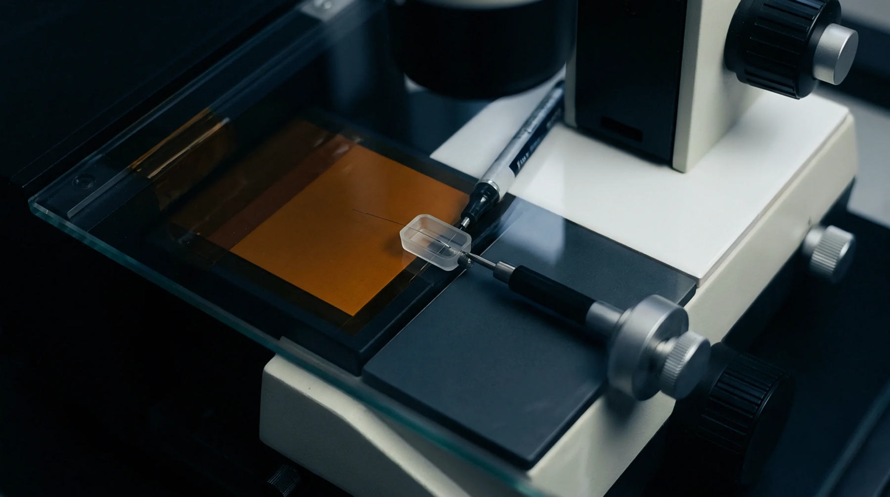
Crystalline characterization techniques analyze the spatial arrangement of atoms within a lattice by measuring the angles of deflected radiation. By measuring lattice spacing, high resolution x-ray diffraction employs monochromatic beams and precise goniometers to assess the strain, composition, tilt and layer thickness of epitaxial films. It identifies the mismatch between a substrate and a layer with sub arcsecond precision, providing data on the crystalline quality of semiconductor materials.
Beam Conditioning
Standard diffraction setups use wide beams, but this specific method utilizes a beam conditioner, such as a crystal monochromator, to reduce wavelength spread and angular divergence. This conditioning ensures that the resulting peaks remain sharp, which is necessary for distinguishing the small shifts caused by lattice deformation. Parabolic mirrors and channel cut crystals further refine the beam profile before it interacts with the sample.
Analysis Mechanism
The instrument measures the intensity of the diffracted x-rays as a function of the angle, producing a rocking curve that displays the distribution of lattice orientations. Precise alignment of the sample in multiple axes ensures that the diffraction condition is met across the entire measurement area. When multiple layers are present, the interference of the waves creates fringes that reveal the exact thickness of the coatings.
This information allows for the calibration of deposition processes and the verification of alloy fractions in complex heterostructures. Automated software routines fit the measured data to theoretical models to extract the physical parameters of the crystal stack. Temperature stability is maintained throughout the measurement to prevent thermal expansion from shifting the diffraction peaks.
Reference Standard
Calibration follows procedures defined by national metrology institutes to ensure that the reported lattice constants are traceable. Drift in the x-ray tube output or thermal expansion of the instrument frame are monitored to prevent measurement errors. Certification of the results confirms that the semiconductor wafer meets the design specification for device performance.