Packaging Technology
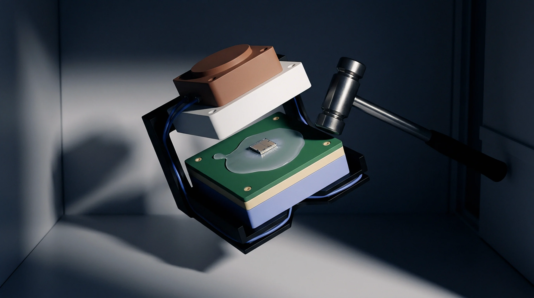
Advanced microelectronic assembly architectures enable the vertical stacking and electrical interconnection of distinct semiconductor materials and functional dies within a single housing. Through this approach, which is referred to as heterogeneous 3d integration, engineers combine sensors, analog circuits, and memory layers processed on different wafer nodes to optimize overall system performance. The resulting multi-die assembly achieves shorter interconnect lengths and reduced parasitics compared to traditional planar configurations.
Thermal Characteristic
Thermal management in densely packed stacked structures requires careful extraction of localized heat. Vertical paths are designed using micro-bumps and through-silicon vias to guide thermal energy toward external sinks. Localized hot spots can quickly degrade performance if heat dissipation is unevenly distributed across the vertical stack.
Assembly Method
Precision manufacturing relies on wafer-to-wafer or die-to-wafer bonding to construct the multi-tiered array. This process demands precise mechanical alignment and controlled bonding forces to secure electrical contacts across the interface. Cleanroom conditions prevent particulate contamination from disrupting the wafer-level adhesion.
Metrological Challenge
Dimensional control and flatness metrics must be monitored throughout the stacking process to prevent die warpage or joint failure. Stress distributions across the bonded layers are measured using micro-Raman spectroscopy to verify structural integrity before final packaging.