Circuit Layout
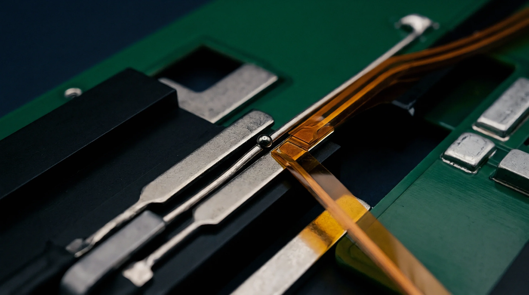
Trace configurations on a printed circuit board minimize the impact of voltage drops by separating high-current lines from voltage-sensing paths. Implementing force and sense terminal routing allows the measurement system to determine the actual potential at the load interface rather than at the connector. This technique is typical in systems requiring high current injection alongside low-level signal detection.
Kelvin Connection
Impedance errors caused by trace resistance disappear when the measurement pair carries negligible current. In force and sense terminal routing the feedback loop compensates for fluctuations in the deliverable voltage. Designers must ensure that the sensing traces run as close as possible to the force traces without creating crosstalk.
Path Isolation
Separation of these specific signals prevents inductive coupling that could disturb the precision of the feedback loop. Effective force and sense terminal routing isolates the noisy return paths from the quiet reference common. Such layouts maintain the integrity of millivolt-level signals in high-density environments.
Verification Standard
Visual inspection and impedance checks confirm that the board fabricator followed the specified trace widths and spacing. When force and sense terminal routing is ignored the resulting errors appear as a gain error that changes with the magnitude of the supply current. Testing rigs verify this behavior during initial power-up.