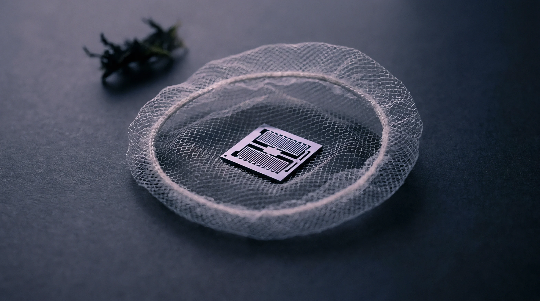
Package Geometry
Surface-mount integrated circuits often utilize a leadless design where the connections are located on the bottom of the plastic body. An exposed pad qfn features a large metal plate in the center of the package that is not covered by the molding compound. It governs the thermal and electrical grounding of the chip to the printed circuit board.
This design provides a low-profile solution for high-density electronic assemblies. The boundary of the package is defined by the outer leads and the dimensions of the central thermal pad. Verification of the pad flatness and the co-planarity of the leads is necessary for a reliable solder connection.
Thermal Management
Dissipation of heat in compact electronic systems is improved by providing a direct path from the silicon to the copper on the board. During the operation of an exposed pad qfn, the central pad is soldered to a corresponding land on the substrate. This mechanism allows thermal energy to flow efficiently out of the package, reducing the junction temperature of the semiconductor.
The size of the pad is optimized to match the heat output of the specific integrated circuit. If the solder bond contains too many voids, the thermal resistance increases and the chip may overheat. Measurement of the thermal performance is verified through infrared imaging or by using internal temperature sensors.
Designers must include thermal vias in the board to conduct heat to the internal copper layers.
Electrical Grounding
High-speed digital and radio frequency circuits require a low-impedance path to the system ground to minimize noise. The exposed pad qfn provides this connection through the large surface area of the central metal plate. This contact reduces the parasitic inductance that would otherwise limit the performance of the device.
The pad is typically connected to the silicon substrate using a conductive die attach material. When the grounding is poor, the circuit may experience instability or electromagnetic interference. Verification of the electrical continuity is performed during the final test phase of the manufacturing process.
Precise alignment of the package during assembly ensures that the pad makes full contact with the board. The measurement of the ground resistance must meet the limits specified in the datasheet.
Manufacturing Tolerance
Fabrication of these packages requires tight control over the molding and lead-finishing processes. An exposed pad qfn must be manufactured with a consistent standoff height to ensure that both the leads and the pad can be soldered successfully. If the pad is recessed too far into the molding compound, it will not touch the solder paste.
Conversely, if the pad is too proud, it may prevent the leads from making contact with the board. These dimensions are verified using automated optical inspection and laser profiling. The precision of the dicing process also impacts the final size and shape of the package.
Any burrs or debris on the edges can interfere with the placement of the component on the assembly line. Regular calibration of the inspection tools ensures that the parts meet the required mechanical specifications.