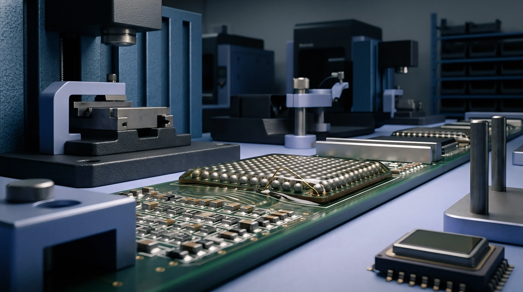
Physical Allocation
Surface area metrics quantify the substrate real estate consumed by an integrated component and its associated pad pattern. The board space footprint dictates package spacing and interconnect routing density across surface mount assemblies. Boundary conditions depend on solder joint inspection access.
Density Boundary
Placement machinery requires mechanical clearance around package bodies to position leads without disturbing adjacent liquidus solder joints. Compressed board space footprint values decrease routing channel availability between component pads, forcing designers to add signal layers to the printed circuit board. Automated optical inspection systems fail when overlapping package courtyards obscure solder fillet profiles.
Clearance Variance
Laser displacement sensors measure actual surface area occupied after automated placement to detect rotational misalignments and component skew. Unintended board space footprint expansion occurs when thermal expansion during reflow pushes flexible lead frames beyond designated pad boundaries. Measurement protocols compare nominal CAD land patterns against physical solder mask openings under calibrated white light illumination.
Precision optical comparators establish absolute spatial location relative to board fiducials. When mechanical tolerances stack unfavorably, adjacent component leads contact neighboring copper fills and create permanent electrical shorts.
Layout Penalty
Thermal dissipation degrades when components pack too tightly onto a common substrate area. Reduced board space footprint restricts ambient convective airflow across power packages, elevating junction temperatures under maximum operational loads. System qualification tests verify package temperature limits under worst-case ambient conditions.