Quantifying On-Chip Reference Buffer Dynamic Impedance Limits during Rapid Transient Current Loadings
On-chip reference buffer output impedance spikes during transient load steps when open-loop gain rolls off, demanding tuned charge-reservoir layout.


Surge
On-chip reference buffers face severe impedance shifts when driven by fast analog-to-digital converter sampling networks. Switched-capacitor input stages draw current pulses with edge rise times under two nanoseconds. During these sampling intervals, the instantaneous current demand spikes from microamperes to tens of milliamperes.
The buffer output stage relies on feedback to maintain constant voltage across the conversion window. At frequencies beyond the unity-gain crossover of the internal operational amplifier, the closed-loop output impedance degrades, transitioning from a fraction of an ohm to several hundred ohms.
Silicon area is limited. Internal compensation capacitors cannot stabilize the loop against instantaneous load steps without slowing the overall settling speed. When an analog front-end samples at five megasamples per second, the reference node has fewer than two hundred nanoseconds to settle within half a least-significant-bit threshold for a sixteen-bit system.
Open-loop output resistance interact with chip-level parasitic capacitance, forming high-frequency poles that alter phase margin during load switching.
At ten megahertz load modulation, open-loop output impedance climbs from zero point eight ohms to forty-two ohms under standard five-volt bias conditions.

Transient Load Step Mechanics in Switched Capacitor Sampling
During the acquisition phase of a successive-approximation-register converter, the internal capacitor array connects directly to the reference pin. The charge stored on the internal array vanishes into the sampling network within the first few nanoseconds. This sudden charge redistribution forces the reference buffer to act as a current source before its active feedback loop reacts.
Buffer bandwidth falls off fast. The initial voltage dip at the reference node depends entirely on the ratio between the internal sampling capacitance and the total bypass capacitance tied to the output terminal. High-frequency AC impedance exhibits inductive peaks where active regulation drops off prior to parasitic capacitance taking over charge delivery.
If the closed-loop bandwidth of the reference driver is twenty megahertz, any current harmonic above this threshold sees an unbuffered impedance determined by interconnect traces and internal silicon metallization resistance.

Closed Loop Open Loop Impedance Phase Shift
Feedback amplifiers alter their impedance characteristics across frequency. At low frequencies, high open-loop gain reduces output impedance to negligible levels. As signal frequency approaches the dominant pole of the amplifier, open-loop gain drops by twenty decibels per decade, elevating output impedance proportionally.
Phase shift across the internal gain stages causes the output impedance to appear inductive across a broad frequency band. When paired with external ceramic capacitors, this inductive characteristic forms a parallel resonant circuit. Resonant peaks elevate impedance at specific transient frequencies, prolonging ringing cycles and corrupting converter linearity.
| Frequency Range | Dominant Impedance State | Typical Resistance (Ω) | Primary Limiting Mechanism |
|---|---|---|---|
| DC to 10 kHz | Closed-loop resistive | 0.05 to 0.20 | Transconductance open-loop gain |
| 10 kHz to 1 MHz | Inductive transition | 0.20 to 8.50 | Amplifier phase margin roll-off |
| 1 MHz to 50 MHz | Peak inductive resonance | 8.50 to 65.00 | Feedback loop propagation delay |
| Above 50 MHz | Capacitive recovery | 2.10 to 12.00 | On-chip interconnect and pad capacitance |
Unbuffered high-frequency current pulses cause code-dependent errors in high-resolution conversion systems. If the reference voltage fails to recover before the comparator makes its final bit decisions, bit errors accumulate systematically. Tuning the output stage demands balancing broad bandwidth against quiescent current consumption on the silicon die.
Reference buffer stability improves when total load capacitance remains strictly within the stability valley defined by the silicon manufacturer.

Bond
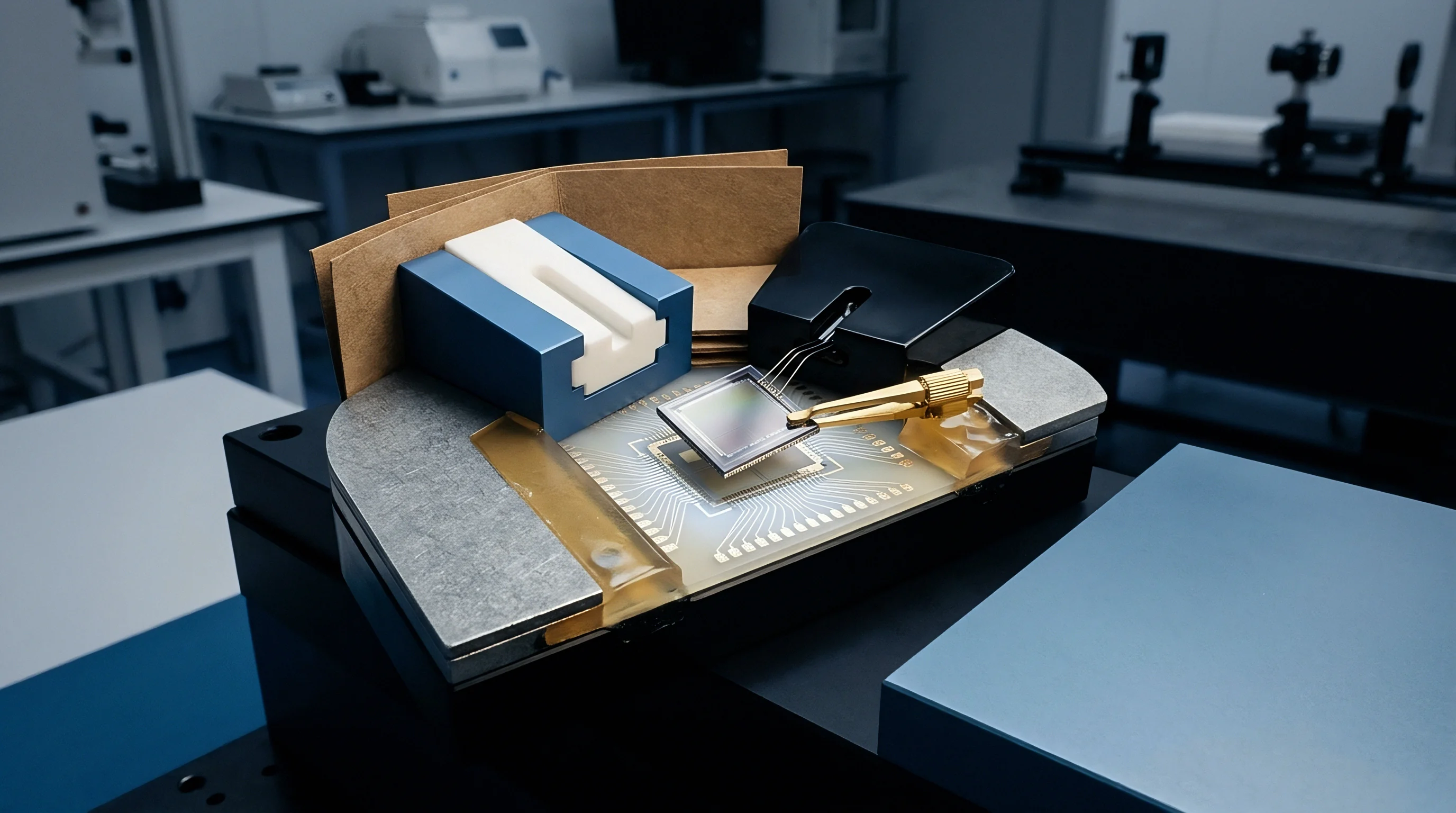
Package leads introduce parasitic inductances that compound the impedance challenge of internal reference circuits. Standard wire-bonded packages present between zero point eight and three point five nanohenries of inductance per package pin. At current slew rates exceeding ten milliamperes per nanosecond, these package inductances induce transient voltage drops that bypass internal chip regulation.
Microscopic wire lengths become primary bandwidth bottlenecks long before signal current reaches the printed circuit board.
Parasitic inductance dominates here. Quad Flat No-Lead packages reduce lead inductance compared to Small Outline Integrated Circuit packages, yet substrate trace paths within the package still restrict high-frequency charge delivery. Flip-chip packaging removes wire bonds entirely, substituting solder bumps with inductances below zero point one nanohenries.
Choosing the package style dictates the upper ceiling of the reference buffer response speed regardless of board-level layout optimization.
Package lead inductance exceeding one point two nanohenries causes reference voltage ringing beyond acceptable limits for AEC-Q100 automotive sensor qualification.

Package Inductances and Pinout Degradation
Inductive coupling between adjacent pins introduces crosstalk from digital control lines into the sensitive reference node. When digital bus lines toggle during a conversion sequence, mutual inductance induces voltage spikes onto the reference pin. Package designs placing the reference pin adjacent to high-speed serial clock lines exhibit measurable degradation in signal-to-noise performance.
Pin placement requires strict isolation strategies. Dedicated ground pins placed on both sides of the reference pin shield the analog node from magnetic field interference generated by adjacent digital switching. Small package footprints like Wafer Level Chip Scale Packaging compress pin pitch to zero point four millimeters, increasing capacitive coupling between adjacent balls unless internal shielding structures are integrated into the silicon substrate.

Silicon Die to Package Substrate Stack Up
The transition from silicon pad to package substrate involves multiple conductor material shifts. Aluminum bonding pads connect to gold or copper wire bonds, which terminate on leadframe posts plated with silver or matte tin. Each interface presents small resistance variations and localized thermal boundaries.
- Wire-bonded QFN16 configuration introduces two point two nanohenries of lead inductance, causing six millivolts of transient droop during two-milliampere load steps.
- Flip-chip CSP assembly reduces package inductance to zero point zero eight nanohenries, limiting transient deviation to under zero point five millivolts under identical load steps.
- Plastic Dual In-Line packaging generates four point seven nanohenries of trace inductance, inducing long ringing tails that require extensive RC damping networks on the board.
- Thin Shrink Small Outline packages display high pin capacitance, shifting the high-frequency pole of the reference buffer feedback loop and reducing phase margin.
Placing a decoupling capacitor without accounting for package lead inductance creates a high-Q resonant circuit that destabilizes the reference output during sudden current steps.

Decay
Settling behavior determines how fast a system resumes conversion cycles following a transient event. When a current step hits the reference buffer output, the initial response includes an instantaneous inductive voltage dip, an amplifier slew-rate recovery phase, and a long exponential tail driven by thermal self-heating within the output transistors. This multi-stage recovery defines the maximum throughput of the data acquisition system.
The voltage droop expands rapidly. If the buffer enters a slew-limited regime, settling times stretch from tens of nanoseconds to several microseconds. Slew-rate limiting occurs when the transient current demand exhausts the internal bias current of the buffer driver stage, forcing internal nodes away from their steady-state operating points.
Decoupling networks must keep peak voltage deviations below thirty microvolts to maintain half-LSB accuracy in high-resolution converters.
Which Rapid Load Step Breaks Reference Voltage Settling?
Load steps exceeding the linear transconductance range of the reference output stage trigger non-linear recovery mechanisms. Small load steps stay within the linear small-signal regime where bandwidth controls settling time. Large current steps exhaust the drive capability of the differential pair within the error amplifier, forcing the circuit into large-signal slew limiting.
Recovery takes several clock cycles. During slew limiting, feedback loops lose control over the output node, allowing internal node voltages to drift. Once the output voltage nears the target value, the amplifier must recover from saturated internal states before resuming linear closed-loop control, causing characteristic overshoots and prolonged settling tails.

Charge Reservoir Sizing and Settling Time
Mitigating reference voltage decay demands an external charge-reservoir capacitor attached directly to the package pin. The reservoir supplies instantaneous current during the first few nanoseconds of a load step, shielding the internal reference buffer from extreme high-frequency demands. The sizing of this capacitor requires balancing transient energy storage against feedback stability limits.
Consider a system built around a sixteen-bit SAR ADC operating at five megasamples per second with an internal sampling capacitor of thirty picofarads. The reference voltage sits at five volts. Each conversion cycle transfers a charge quantity calculated by multiplying the reference voltage by the sampling capacitance, yielding one hundred fifty picocoulombs per sample.
If this charge must be drawn within a ten-nanosecond acquisition window, the instantaneous current reaches fifteen milliamperes.
To limit the voltage drop to less than half a least significant bit (which equals thirty-eight microvolts for a five-volt sixteen-bit system), the total decoupling capacitance tied to the reference pin must satisfy the ratio of total transferred charge to maximum allowable voltage change. Dividing one hundred fifty picocoulombs by thirty-eight microvolts yields a minimum required external reservoir capacitance of three point nine five microfarads. Selecting a standard four point seven microfarad ceramic capacitor provides a small safety margin.
- Calculate the maximum charge transfer per acquisition cycle based on sampling capacitance and reference voltage.
- Determine the maximum allowable voltage drop corresponding to half of one least significant bit of the target converter resolution.
- Compute the required minimum reservoir capacitance by dividing charge transfer by maximum allowable voltage drop.
- Select a ceramic capacitor value exceeding the calculated minimum while staying below the amplifier upper stability limit.
- Verify the equivalent series resistance of the selected capacitor to prevent high-frequency parasitic ringing.
Thermal tails shift offset voltages. When high transient currents flow through the output stage of the reference buffer, localized thermal gradients develop across the silicon die. These thermal gradients alter the threshold voltages of matched transistor pairs within the reference bandgap core, causing slow DC voltage drifts that persist long after the electrical transient has cleared.
Silicon suppliers frequently explain settling tail degradation as an unavoidable artifact of board-level ground loops rather than internal buffer bias shift.


Channel
Digital interface busses operating alongside sensitive reference lines present direct interference paths into analog signals. High-speed SPI or I2C clock lines carrying sharp logic edges generate magnetic and electric fields that couple into high-impedance reference traces. As bus speeds increase to fifty megahertz, edge transition rates under one nanosecond inject significant high-frequency noise into adjacent analog channels.
Placement geometry alters loop gain. Routing digital signal traces parallel to the reference buffer output line creates parasitic capacitance between the conductors. Every logic transition transfers a tiny charge packet through this parasitic capacitance into the reference node, driving the reference buffer out of its linear operating region.
Trace isolation gaps under zero point five millimeters allow digital bus crosstalk to degrade analog converter signal-to-noise ratio by up to twelve decibels.

Digital Bus Activity and Reference Line Crosstalk
Serial bus communication often occurs concurrently with analog sampling cycles. Burst transfers over SPI busses create periodic supply current surges within the host microcontroller, causing system ground potential variations. These ground shifts modulate the reference buffer ground return pin, creating differential noise at the analog reference input.
Land pattern parasitics add up. Differential routing of reference lines combined with dedicated ground return channels suppresses common-mode bus noise. Separating digital logic supplies from analog reference supplies prevents switching noise on digital power rails from corrupting the internal bias networks of the reference generator.

Clock Edge Coupling across Package Leadframes
Leadframe structures in integrated circuits introduce capacitive coupling between pin channels. A serial clock pin adjacent to an analog reference pin forms a parasitic coupling capacitance of approximately zero point two picofarads through the package plastic mold compound.
| Interface Type | Package Style | Pin Isolation Strategy | Crosstalk Attenuation at 50 MHz |
|---|---|---|---|
| SPI (4-wire) | SOIC-16 | No guard pins | -28 dB |
| SPI (4-wire) | QFN-24 | Single ground guard pin | -44 dB |
| I2C (Fast Mode) | TSSOP-20 | Shared ground plane | -32 dB |
| Parallel Bus | LGA-48 | Dedicated shield trace channel | -58 dB |
Shielding layout requires strict enforcement during schematic capture and printed circuit board routing. Installing guard rings around reference traces diverts surface leakage currents and high-frequency electric fields away from the sensitive reference node into a quiet analog ground point.
System designers maintain compliance by integrating structural isolation rules into their design checklists.
- Guard ring placement completely surrounding the reference pad prevents surface leakage currents on dirty circuit boards from corrupting precision node voltages.
- Orthogonal bus routing where digital traces cross analog reference lines at ninety-degree angles minimizes capacitive and inductive cross-coupling.
- Ground plane splits isolating dirty digital ground returns from clean analog reference ground returns prevent ground bounce corruption.
- Series damping resistors added to digital bus lines slow down clock edge rates, reducing high-frequency electromagnetic radiation into reference circuits.
Standard IPC-2221A Section 10.1 specifies minimum conductor spacing requirements to prevent electrical breakdown and control signal crosstalk in high-density interconnect assemblies.

Ledger
Choosing between integrated reference buffers and standalone external buffer solutions alters both component cost and board assembly complexity. An on-chip reference buffer saves board real estate and eliminates an extra surface-mount component from the bill of materials. Integrating the buffer onto the main converter die increases silicon die size, lowers manufacturing yield, and raises unit component price.
Board spin cycles add cost. When an integrated reference buffer fails to meet system settling specifications under dynamic transient loading, redesigning the printed circuit board to add an external driver inflates project expense. External operational amplifiers optimized for capacitive load driving cost between zero point forty and two point ten US dollars in volume quantities, adding direct component expense while demanding additional power rail decoupling.
Moving from an internal buffer to a dedicated external precision driver increases total solution bill-of-materials cost by zero point sixty-five dollars per channel.

Delivered Unit Cost versus External Buffer Component Count
Commercial evaluations must account for total landed manufacturing costs rather than silicon unit price alone. Integrating a high-performance buffer requires larger transistor geometries and specialized analog process options inside the silicon foundry. These additions increase overall die cost across all production volumes.
Firmware delays increase unit expense. Troubleshooting reference settling instabilities late in product development pushes back production release dates, incurring revenue losses. Using bare die options or wafer-level chip-scale packaging cuts silicon footprint but elevates assembly line handling risks and board yield losses.
| Implementation Path | Unit BOM Cost (10k pcs) | Board Area Overhead | Assembly Line Yield Risk |
|---|---|---|---|
| Integrated On-Chip Buffer | $0.00 (Base die cost) | 0 mm² | Low (Single component) |
| External Precision Op-Amp | $0.48 – $1.25 | 12 – 25 mm² | Low (Standard SMT) |
| Dedicated Voltage Reference IC | $0.85 – $2.40 | 18 – 35 mm² | Low (Standard SMT) |
| Discretely Buffered Reference | $0.32 – $0.75 | 30 – 60 mm² | Medium (Multiple placements) |
Solder voiding worsens thermal paths. When using bottom-terminated packages like QFNs for high-current reference drivers, solder voiding underneath the thermal pad impairs heat dissipation, inducing thermal gain drift over time. Qualification protocols must inspect thermal pad voiding percentages to maintain long-term calibration stability.
Direct pin routing lowers drop. Placing the external buffer within three millimeters of the converter reference input pin cuts trace inductance, ensuring maximum transient regulation capability.
Whether future sub-micron CMOS manufacturing processes can successfully integrate wideband reference buffers without sacrificing die yield or introducing severe thermal tail effects remains an open question for system architects balancing performance against production budget limits.