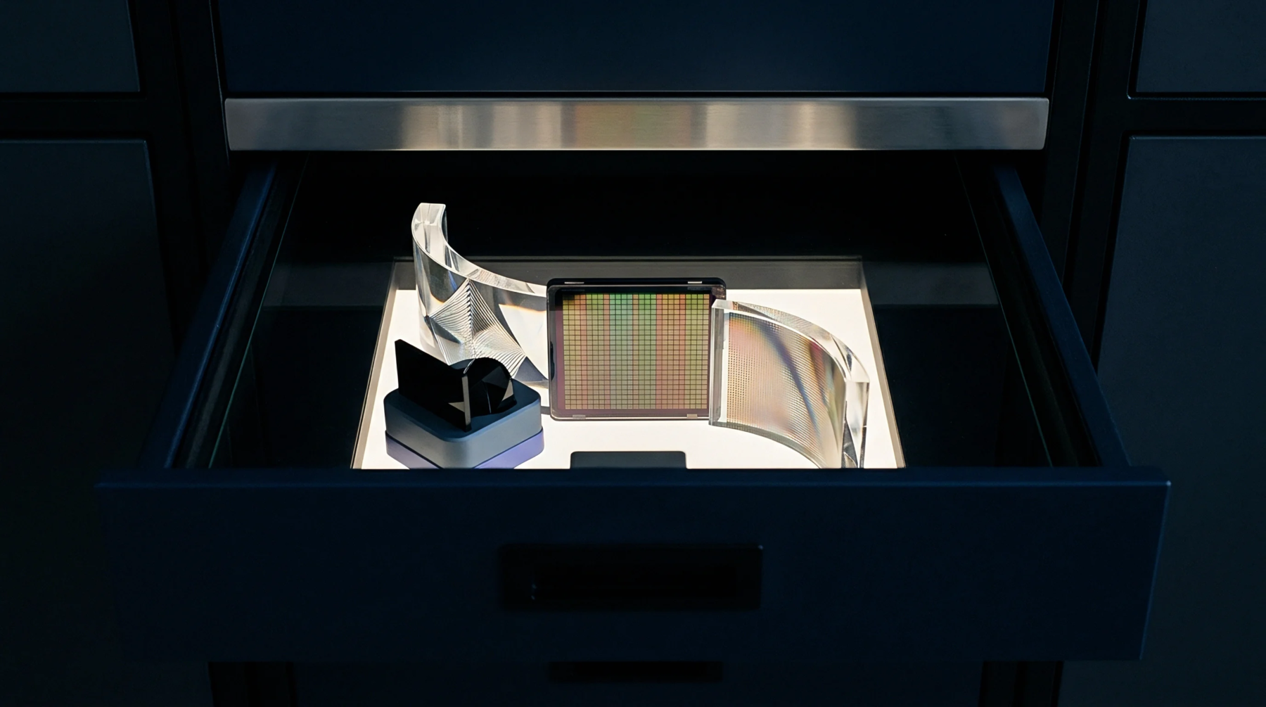
Surface Distortion
Aggregate mechanical tension across a semiconductor disc arises during high-temperature processing steps and influences the flatness of the entire surface. Wafer level stress accounts for the cumulative effect of all thin film layers and thermal cycles on the mechanical stability of the disc. If this tension is not balanced, the wafer will warp into a shape that prevents it from being processed by automated equipment.
This can lead to cracks during dicing or poor focus during lithography.
Layer Stack
Every new material added to the wafer contributes its own internal pressure. Wafer level stress is the sum of these individual forces, which can either cancel each other out or add together. Engineers often use a compensating layer on the back of the wafer to counteract the pull of the front-side circuits.
Laser Profilometry
Measuring the surface profile involves scanning a laser beam across the diameter of the disc. The resulting map shows the peaks and valleys caused by wafer level stress. This data is used to adjust the deposition parameters in real time.
Lithographic Overlay
Precise alignment of multiple mask layers requires a perfectly flat substrate. When wafer level stress causes the surface to bend, the alignment marks no longer match the projection. This distortion limits the minimum feature size that can be produced on the chip.