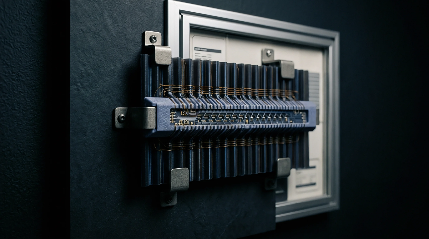
Temperature Coupling
Physical transfer of operational heat from dissipating circuit elements back into temperature-sensitive input stages alters internal operating points, biasing thresholds, and transfer characteristics. Unintended thermal feedback introduces parasitic internal loops where output power shifts induce localized substrate temperature gradients that drift baseline amplifier offset voltages and gain coefficients. In monolithic power operational amplifiers or multi-transistor arrays, heat generated in output stages conducts across the silicon die to the differential input pair, introducing low-frequency distortion and baseline drift.
The phenomenon occurs in any electronic, optical, or electrochemical assembly where temperature-dependent operating parameters are subject to the thermal consequences of their own output actions. Its analytical boundary is bounded by the physical thermal resistance and thermal time constants connecting the heat-generating source to the affected sensor or input circuit.
Substrate Interaction
Heat conduction through silicon occurs rapidly across short microscale distances, establishing transient spatial gradients across integrated circuits. An asymmetric layout allows the output transistor pair to heat one input transistor more than its matched companion, producing a false input-referred differential error voltage. This thermal transfer function acts as an internal feedback network operating in parallel with designed electrical feedback loops.
Because thermal diffusion through silicon and copper packaging exhibits low-pass filter characteristics with corner frequencies typically below a few hundred hertz, this parasitic interaction alters open-loop phase margins exclusively at low frequencies, creating low-frequency gain peaking or anomalous phase shift.
Measurement Vulnerability
Precision direct-current instrumentation amplifiers and precision voltage references are exceptionally susceptible to internal thermal feedback anomalies. Output load changes vary internal device power dissipation, driving thermal gradients across internal bandgap reference junctions and precision thin-film resistor networks. The resulting output drift can mimic true physical measurement changes, ruining calibration accuracy in low-level transducer interfaces.
Board-level layout contributes similar degradation when external power regulators or power stages share copper ground planes with sensitive signal acquisition front-ends.
Layout Suppression
Mitigating parasitic thermal loops requires layout techniques that equalize heat distribution across critical circuit elements. Cross-coupled quad layouts for differential transistor pairs cancel linear thermal gradients by balancing heating across four diagonally opposed active areas. Placing heat-dissipating power drivers along the central thermal symmetry axis prevents asymmetrical heating of balanced input channels.
Packaging designs integrate thick copper heat slugs and low-thermal-resistance thermal vias to rapidly pull operational heat directly out through the substrate into external sinks, preventing lateral heat spread across sensitive operational nodes.