Thermal Stress
Mechanical deformation of sensor packaging occurs during the high-temperature solder reflow assembly process. As the printed circuit board cools, post-reflow offset drift introduces persistent mechanical stresses that shift the electrical baseline of sensitive analog components. This drift can significantly degrade the initial accuracy of pre-calibrated sensors once they are mounted on the system board.
Design engineers must characterize this shift to ensure the system meets its overall accuracy budget.
Assembly Impact
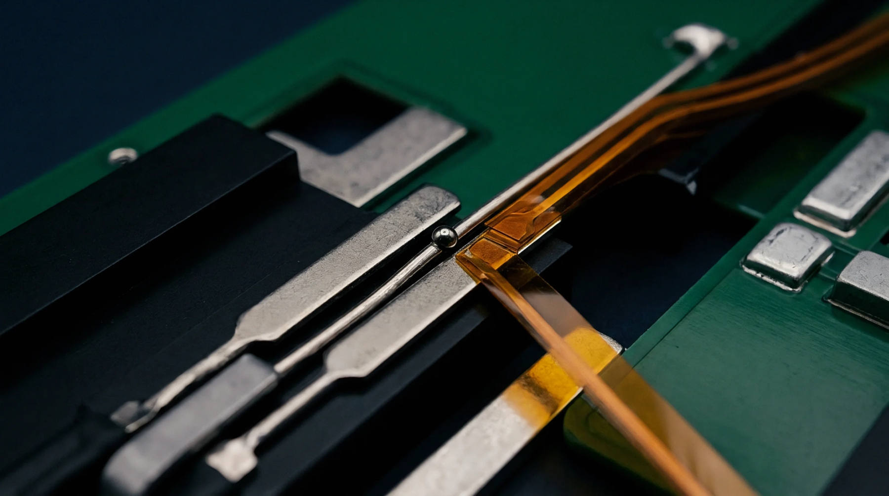
Solder alloy solidification and thermal contraction of the circuit board exert non-uniform mechanical forces on the sensor housing. These forces are transmitted directly to the silicon die, causing localized piezoresistive stress and shifting the calibration of internal amplifiers and bridge circuits. To minimize this post-reflow offset drift, board designers often utilize thin-film substrates or incorporate isolation slots around the sensor.
In addition, using low-temperature solder alloys or controlled cooling profiles can reduce the residual stress locked into the assembly.
Longterm Behavior
Stress relaxation occurs slowly over time as the circuit board and packaging materials adjust to their post-assembly state. This slow relaxation can cause the offset to drift further over several days or weeks after assembly. System designers often implement a burn-in phase or a late-stage calibration step to allow these stresses to stabilize before the final system test.
Layout Optimization
Layout optimizations can isolate the sensitive component from board-level stresses. Positioning the sensor far from mounting screws, connector pins, and heavy components reduces the mechanical strain transmitted through the board.