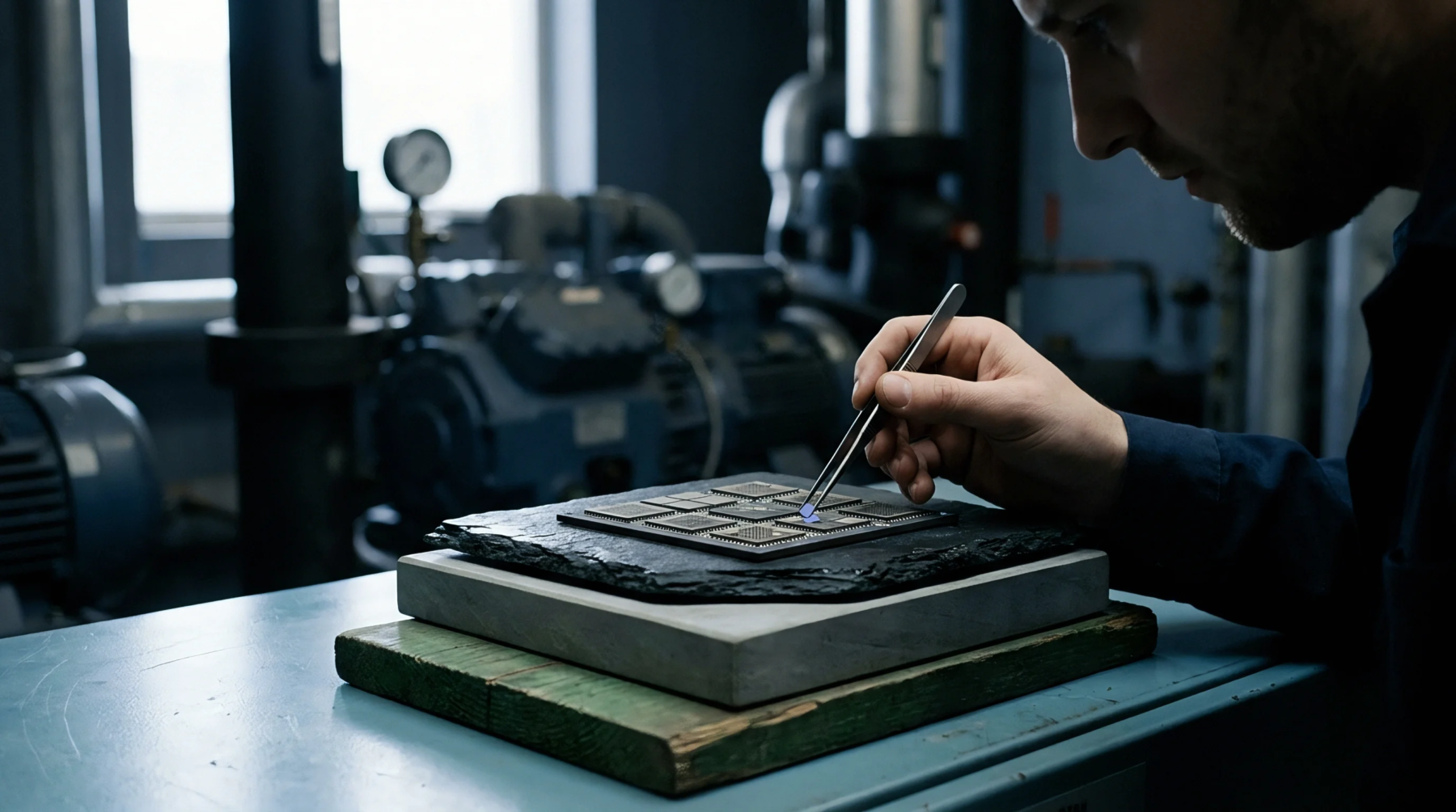
Physical Separation
Machined slots routed through printed circuit board substrates prevent surface leakage currents and improve high-voltage creepage insulation. Removing dielectric substrate material between conductive pads eliminates physical surface tracking paths. Implementation of a PCB cutout trench increases effective isolation distance across high-voltage insulation boundaries.
Structural limits apply where mechanical board integrity becomes compromised by physical routing slots.
Isolation Channel
High potential differences across board surfaces create tracking risks where contamination or condensation lowers dielectric breakdown resistance. Air gaps provide significantly higher dielectric strength than contaminated glass-epoxy circuit board laminate surfaces. Routing mechanical slots between primary and secondary circuit regions forces arc paths to traverse air rather than board surfaces.
System designers use milled channels to satisfy safety agency clearance requirements without increasing board surface area. Airborne particulate deposition inside narrow trenches reduces long-term insulation effectiveness if dust accumulation occurs in humid environments.
Structural Boundary
Panel design routines define tool bit diameters and tab placements for milled slots. Milling tools create rounded inner corners that concentrate mechanical stress during board depaneling or vibration testing. Copper plane clearances along trench edges prevent exposed trace edges from shorting during routing operations.
Inner layer copper pullback distances ensure adequate dielectric spacing around cutout perimeters.
Manufacturing Tolerance
Routing bit positional accuracy determines the dimensional variance of substrate cutouts. Unintended solder bridging can bridge narrow slots during wave soldering operations. PCB cutout trench dimensions dictate minimum air clearance compliance in compact power converters.