Contact Physics
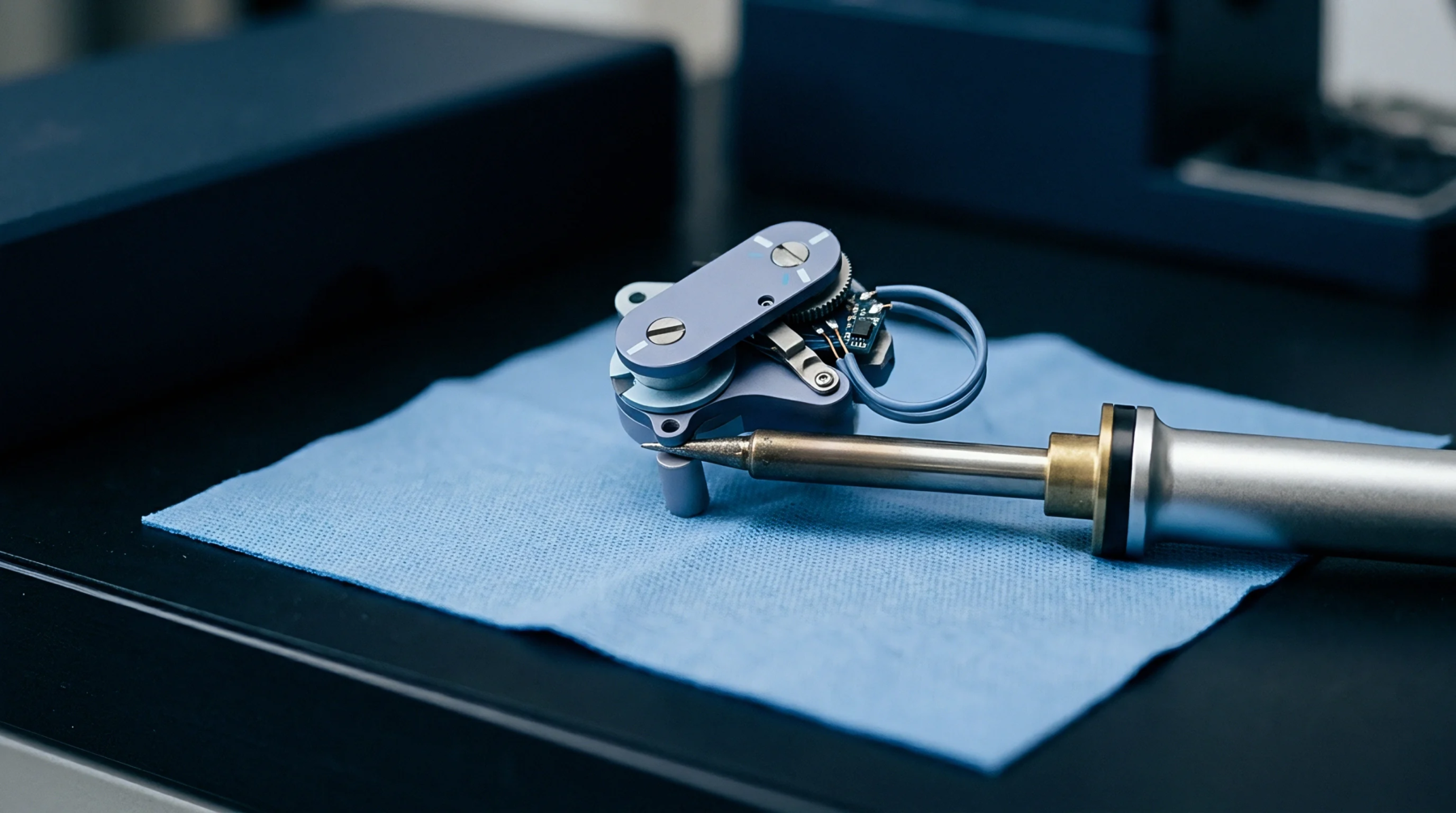
Precision positioning mechanisms drive sub-micron needle tips onto miniature test pads to establish direct electrical contact with integrated sensor circuitry prior to packaging. Diagnostic signal acquisition during early wafer qualification relies on micro-probing to measure transistor threshold voltages and trace resistance without damaging sensitive die dielectrics. Contact resistance must remain stable below one ohm across hundreds of touchdowns.
Overdrive distance controls needle skate across the aluminum or copper pad surface to pierce native oxide layers. High-density pads require tungsten or beryllium-copper probe tips shaped with tip radii under five micrometers.
Parasitic Capacitance
Coaxial and triaxial probe cables shield high-impedance measurement nodes from stray electromagnetic fields. Physical proximity of needle shanks during micro-probing introduces parasitic capacitance ranging from tens of femtofarads to several picofarads. Driven guard circuits neutralize stray capacitive currents during low-level picoampere leakage measurements.
Calibration Protocol
Wafer-level calibration standards on alumina substrates calibrate vector network analyzers up to millimeter-wave frequencies. Precision alignment algorithms compensate for thermal drift of the probe station stage while micro-probing maintains tip location over multi-hour qualification sequences. Standard short-open-load-thru procedures correct for system phase shifts up to sixty gigahertz.
Operational Limit
Physical pad size reduction below ten micrometers and extreme environmental temperature testing define the boundaries of mechanical probe contact integrity. Thermal expansion of probe arms during hot-chuck testing alters contact force, while micro-probing on ultra-low-k dielectrics risks subsurface cracking if skate force exceeds three grams per tip. Final compliance testing verifies pad oxide thickness after probe mark inspection.