End of Life Notices That Take One Package and Spare Another
When component vendors end leaded packages, identical active silicon dies often survive in surface-mount forms that demand revised land patterns and thermal layouts.
Metal structures provide the mechanical support and electrical connectivity for an integrated circuit die within a protective plastic or ceramic housing. The leadframe packaging process starts with a thin sheet of copper alloy or iron nickel that has been etched or stamped into a specific pattern of leads and a central die paddle. This frame acts as the skeleton of the semiconductor device, providing the external pins that connect the chip to a printed circuit board.
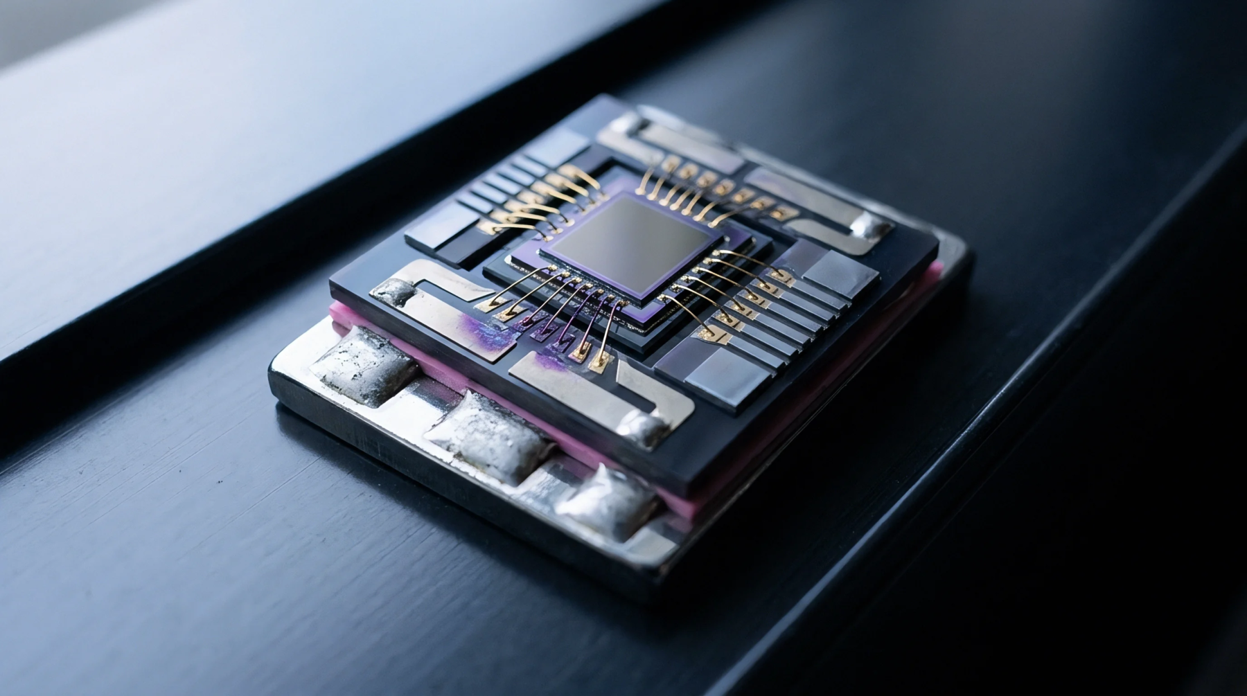
During assembly, the silicon die is bonded to the central paddle using an adhesive or a metallic solder. The leads are then connected to the contact pads on the die using thin gold or aluminum wires. This traditional packaging style remains the most widely used format for low to medium pin count devices due to its low cost and high reliability.
Bonding of the semiconductor crystal to the metal frame is a critical step that determines the thermal and mechanical stability of the final product. The die attach material must provide a strong physical bond while also allowing for the different rates of thermal expansion between the silicon and the leadframe. Most manufacturers use an epoxy resin filled with silver particles to ensure high electrical and thermal conductivity.
For high power applications, a eutectic solder or a silver sintering process is used to create a more robust thermal path. Once the die is secure, the wire bonding process creates the electrical paths that allow the signal to flow from the silicon to the external world. This assembly is then encapsulated in a plastic molding compound to protect the delicate internal components from moisture and physical damage.
Electrical paths within the package are formed by the leads which extend from the internal bond zone to the outside of the plastic body. These leads can be formed into various shapes, such as the gull wing style used in small outline packages or the flat pads found in leadless designs. The geometry of the leads affects the parasitic inductance and capacitance of the device, which in turn influences its high frequency performance.
Copper leadframes are preferred for their superior thermal and electrical properties, while iron nickel alloys are chosen for their strength and compatibility with certain glass to metal seals. The surface of the leads is typically plated with a layer of tin or a combination of nickel, palladium and gold to ensure good solderability.
Protection of the internal circuitry from environmental stress is the primary function of the molded body that surrounds the leadframe. The plastic molding compound must have a coefficient of thermal expansion that is closely matched to the metal frame to prevent cracking or delamination during temperature cycling. Leadframe packaging provides a rugged and cost effective solution for a vast range of consumer, industrial and automotive applications.
Despite the rise of more advanced flip chip and wafer level technologies, the leadframe remains a staple of the semiconductor industry. It offers a proven balance of performance and manufacturability that is difficult to beat for standard electronic components.
When component vendors end leaded packages, identical active silicon dies often survive in surface-mount forms that demand revised land patterns and thermal layouts.
Expertise is a utility, not a secret. sentiention™ publishes its working knowledge as open reference: intelligence layer covering the materials it sources, the markets it enters, and the reference that serves both.