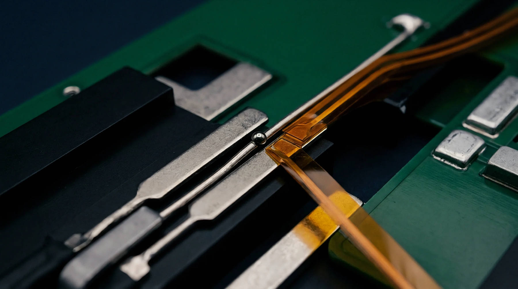
Measurement Arrangement
Four-terminal conductor topologies eliminate lead and contact resistance errors by separating the current-carrying circuit from the voltage-sensing circuit. A true kelvin contact applies source excitation through one discrete pair of leads while high-impedance sense instruments measure potential drop across the remaining pair. The sensing loop draws negligible current, which suppresses the potential drop across the measurement lead resistances and contact interfaces.
This geometry operates across low-resistance metrology from sub-milliohm shunt resistor calibration to automated wafer-level semiconductor parameter testing. The four-wire isolation ceases to provide accurate voltage readings when leakage paths between adjacent leads bypass the input impedance of the measuring voltmeter.
Resistance Compensation
Extraneous circuit resistances drop out of the governing measurement equation through physical branch separation. Current forced through outer force conductors encounters source line impedance, test socket resistance, and probe tip contamination without affecting the inner sense branch. Instrumentation amplifiers inside the voltage meter present input resistances exceeding ten gigaohms, which restricts sense current to picoamp levels.
The resulting potential drop across the kelvin contact sense interfaces remains below the microvolt noise threshold of the detection electronics. Lead resistance variations caused by ambient temperature swings or cable flexion cancel out during signal processing. Parasitic offset voltages from thermoelectric Seebeck effects cancel out when dual-polarity current reversal testing sequences run consecutively.
Interface Verification
Mechanical alignment of twin probe tips governs the repeatability of micro-ohmic measurements on fine-pitch pads. Wear across the tip faces of a kelvin contact increases contact resistance on the force pathway, driving compliance limits on precision current sources. Sensor verification requires periodic zero-resistance nulling against certified gold-plated planar shorting blocks.
Particulate accumulation between co-axial or bifurcated probe tips causes unintended bridging between force and sense conductors, converting four-wire circuits into conventional two-wire networks. Contact force must remain within specified mechanical limits, typically between fifteen and fifty centinewtons per tip, to breach non-conductive surface oxide films. Planarization drift between paired probe needles introduces contact skew, altering the exact spatial point of voltage detection on small test structures.
Parasitic Degradation
Alternating-current measurements introduce inductive coupling between parallel force and sense conductors that degrades low-impedance readings. Mutual inductance across adjacent conductor paths in a kelvin contact injects an error voltage proportional to frequency and excitation current. High-frequency applications require twisted-pair shielding or coaxial leads right up to the probe tips to isolate the sense loop.
Common-mode voltage errors arise when the potential difference between the device under test and instrument ground exceeds input rejection ratios. Dielectric insulation resistance between force and sense traces must exceed several gigohms to prevent shunt leakage currents from distorting microvolt-level potential drops. Extreme magnetic fields induce eddy currents in surrounding metallic test fixtures that distort the measured low-impedance potential field.