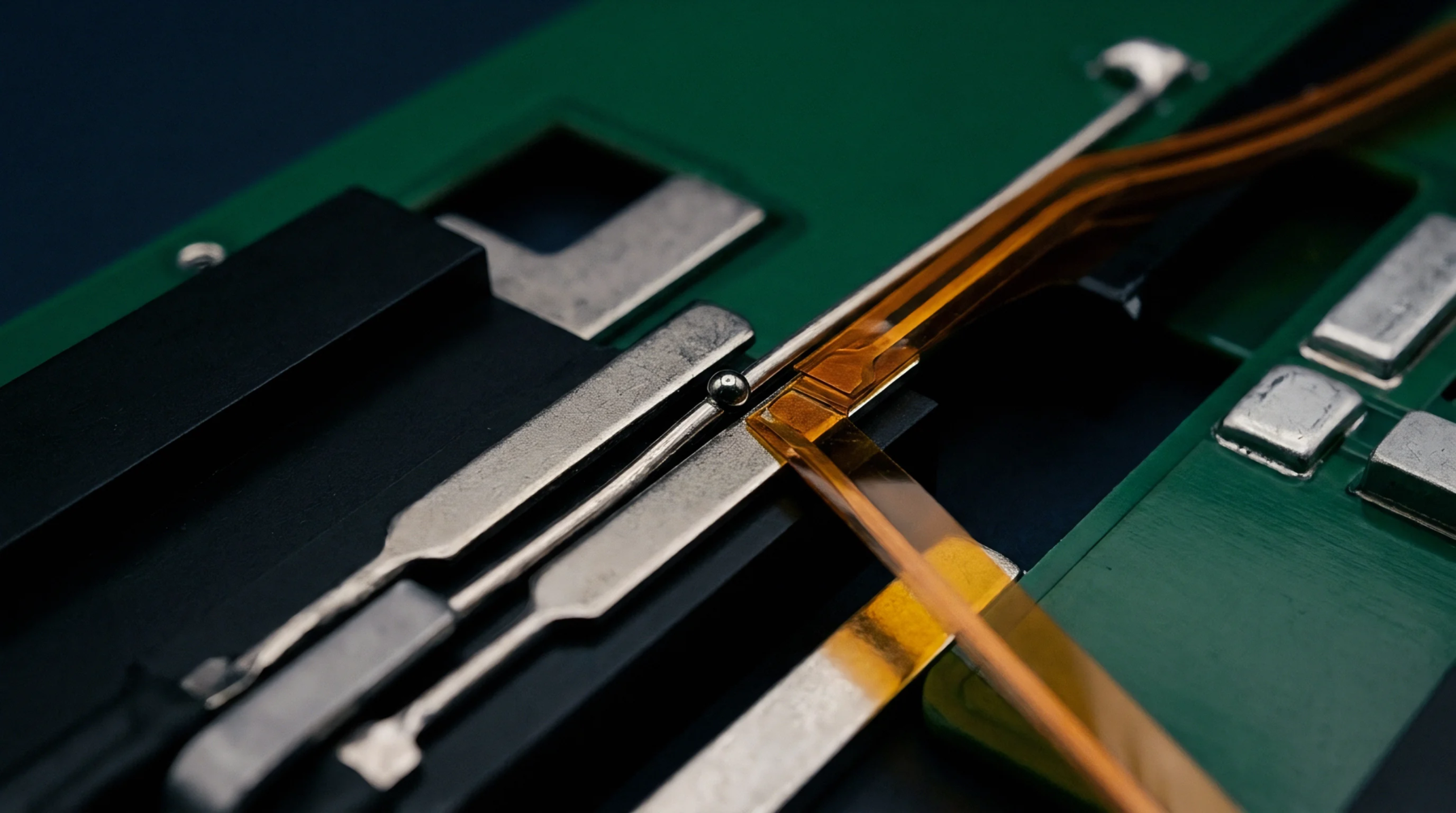
Precision Analog Converter Gain Drift under Dynamic Thermal PCB Stress
Dynamic PCB thermal gradients cause substrate flexing that alters converter resistor ladder ratios via piezoresistive strain, driving gain drift.
Implementation guidance for surface mount design requires structured evaluation methodologies to bridge component geometry with assembly yield limitations. IPC J-STD-012 establishes the technical framework for determining board layout patterns that survive thermal excursions during reflow soldering. Metrological evaluation against this document relies on exact land pattern dimensions, heel fillets, and toe fillets verified under optical magnification at standard ambient reference conditions.
Production facilities verify compliance by comparing measured joint volumes against established limits, ensuring that bridging and insufficient solder are avoided. Thermal cycling induces mechanical stress at the interface between the component termination and the printed circuit board pad, meaning that geometric conformity controls the rate of fatigue accumulation.
Assembly process qualification depends on separating variations driven by solder paste deposition from those caused by substrate design flaws. Positional accuracy of the printing equipment introduces offset errors that degrade joint formation regardless of pad geometry precision. Calibration of stencil printers involves adjusting squeegee pressure and separation speed to maintain deposit repeatability, which isolates layout defects from machine-induced anomalies.
Environmental chamber testing exposes finished assemblies to thermal shock profiles, revealing interfacial degradation that static inspection procedures cannot detect. Tolerances defined within the document apply strictly to nominal conditions prior to environmental stress application, and any post-test deviation indicates material fatigue rather than initial manufacturing non-conformance.
Solder joint integrity degrades when operational temperatures exceed the glass transition temperature of the laminate material, altering the mechanical compliance of the interconnection. Thermal expansion mismatch between ceramic chip carriers and FR-4 substrates generates shear forces across the solder fillet, leading to microcracking over extended duty cycles. Verification benches measure resistance fluctuations during rapid temperature transitions to quantify electrical continuity degradation in real time.
Instrument drift within thermal chambers can compromise the accuracy of environmental stress screening, requiring periodic calibration using certified thermocouple references to maintain measurement validity. Operator intervention is prohibited during automated data collection cycles to prevent manual interference from masking true material response characteristics.
Manufacturing throughput relies on minimizing defect rates through rigorous control of paste release characteristics and reflow profile optimization. Peak temperature settings during infrared reflow must remain within a narrow thermal window to activate flux chemistries without damaging heat-sensitive semiconductor packages. Calibration of conveyor speed and heating zone thermocouples ensures that board surface temperatures match the theoretical profile required for complete intermetallic compound formation.
Inspection systems evaluate fillet heights using laser displacement sensors to verify that solder volume meets minimum structural requirements without exceeding bridging thresholds. Process yields improve when layout engineers align land patterns directly with the specific packaging geometry dictated by the production specification.
Dynamic PCB thermal gradients cause substrate flexing that alters converter resistor ladder ratios via piezoresistive strain, driving gain drift.
Expertise is a utility, not a secret. sentiention™ publishes its working knowledge as open reference: intelligence layer covering the materials it sources, the markets it enters, and the reference that serves both.