Decoupling Capacitor Selection for Precision Analog Reference Inputs
Precision reference input decoupling requires Class 1 C0G dielectrics and sub-nanohenry loop inductance to prevent microphonic noise and voltage droop.


Dielectric
Class 1 ceramic formulations maintain capacitance stability across terminal voltage variations, whereas Class 2 ferroelectric compounds lose up to eighty percent of their rated storage when biased near operational limits. Silicon references drift under board flex. In precision conversion circuitry, the reference input pin represents a dynamic load that directly modulates the analog-to-digital transfer function.
Capacitance variations at this node alter circuit impedance, translating directly into gain error and integral nonlinearity across the conversion range.
Piezoelectric Response and Voltage Coefficient Dynamics
Mechanical vibration converts directly into electrical noise inside barium titanate crystal structures through inverse piezoelectric action. Class 2 formulations such as X7R and X5R exhibit high microphonic sensitivity, generating sub-millivolt electrical spikes when subjected to mechanical shock, acoustic pressure, or board strain from thermal expansion. C0G dielectrics, fabricated from calcium zirconate or neodymium oxides, lack domain wall movement under stress and show zero measurable piezoelectric response down to the nanovolt noise floor.
Low dielectric absorption prevents memory errors.
Voltage coefficient of capacitance presents a severe error mechanism in surface-mount ceramic packages. A 10 μF X7R capacitor in an 0603 package size loses approximately 65 percent of its nominal value when operated at a 5 V DC bias. Increasing the physical package size to 1206 restores dielectric thickness between electrode layers, reducing capacitance loss to 15 percent at the same 5 V bias.
C0G capacitors maintain their full rated capacitance across their entire rated working voltage range without voltage-dependent attenuation.
| Dielectric Material | Capacitance Drift (-55°C to +125°C) | DC Bias Loss at 5V (0805 Package) | Dielectric Absorption | Leakage Current Density (nA/μF) |
|---|---|---|---|---|
| C0G / NP0 Ceramic | ±30 ppm/°C | 0.0 % | 0.01 % | 0.05 |
| X7R Ceramic | ±15.0 % | -45.0 % | 0.60 % | 1.20 |
| Polyphenylene Sulfide (PPS) Film | ±1.5 % | 0.0 % | 0.05 % | 0.10 |
| Hermetic Tantalum Polymer | ±10.0 % | 0.0 % | 0.15 % | 5.00 |
Dielectric Absorption and Insulation Resistance Shift
Residual charge retention inside the insulator material produces voltage memory effects after rapid step changes at the converter input terminal. Dielectric absorption, quantified as the recovery of charge after short-circuit discharge, causes reference node voltage tailing. X7R materials display dielectric absorption values between 0.5 percent and 1.0 percent, creating long settling tails that degrade 18-bit and 24-bit conversion accuracy.
C0G formulations yield dielectric absorption below 0.01 percent, enabling complete voltage settling within sub-microsecond acquisition windows.
A C0G ceramic capacitor maintains less than 0.1 percent capacitance variation across an operating temperature range of minus 55 to plus 125 degrees Celsius.
Insulation resistance decreases exponentially with elevated operating temperature. Lower insulation resistance raises steady-state leakage current entering the reference pin node, introducing fixed offset errors across high-impedance source networks. Thermally induced leakage drift in Class 2 ceramics alters DC accuracy over extended industrial operating sweeps, whereas Class 1 dielectrics maintain insulation resistance values exceeding 100 gigohms up to 125 degrees Celsius.
Manufacturers frequently defend high voltage coefficients in small ceramic packages by noting that volume-constrained assembly lines prioritize volumetric efficiency over voltage linearity.

Charge
Switched-capacitor input networks in high-resolution analog-to-digital converters demand instantaneous current bursts during each conversion cycle. Bias voltage degrades effective capacitance. When internal switches connect the sampling array to the reference input, charge transfers from the local external decoupling node into the internal capacitor array within nanosecond windows.
Inadequate localized energy storage forces the reference buffer to deliver sudden current transients, inducing transient voltage droop at the converter reference terminal.
Transient Dynamic Current Profiles in Precision Converters
Successive approximation converters toggle internal switch matrix arrays that draw current pulses reaching tens of milliamperes within window intervals under two nanoseconds. Charge demands spike during conversion. The peak dynamic current scales with clock frequency, internal array capacitance, and input signal amplitude.
Delta-sigma modulators generate continuous high-frequency switched-capacitor dynamic loads, producing cyclic ripple on the reference rail that folds back into the baseband spectrum as intermodulation distortion if unsuppressed.
Class 1 ceramic bypass components specified under MIL-PRF-55681 mandate maximum equivalent series resistance limits to guarantee transient settling times below 50 nanoseconds.
- Reference Voltage Droop occurs when the local capacitor fails to replenish the switched internal matrix before the converter latches its comparator output.
- Amplifier Ringing Dynamics emerge when excessive capacitive loading pushes the reference driver phase margin below thirty degrees, causing prolonged voltage oscillations.
- Inter-Bit Crosstalk Errors develop when residual transient noise from one bit decision corrupts the reference voltage available for subsequent bit decisions.
- Gain Thermal Drift accumulates as high peak current pulses generate localized self-heating inside internal amplifier output stages.
Reference Buffer Stability and Compensation Loop Limits
Operational amplifiers driving reference pins risk severe phase margin erosion when loaded by high-value ceramic reservoirs without series damping. High buffer loop gain causes ringing. Large output capacitance introduces a secondary pole in the amplifier feedback loop, degrading phase margin and producing underdamped transient responses to dynamic current steps.
Inserting a small physical series resistor between the buffer output and the decoupling capacitor isolates capacitive loading while maintaining low DC output impedance.
Series resistance stabilizes the amplifier loop. The isolator resistance value must balance control loop stability against dynamic voltage drop during high-speed sampling phases. An optimal resistance value matches the equivalent series resistance needed to achieve critical damping without extending the voltage recovery time beyond the available acquisition period.
Selecting inadequate reservoir components causes unrecoverable conversion nonlinearity, degrading the effective number of bits by up to 3 LSBs in 18-bit architectures.
Parasitics
Trace inductance between a reservoir component and the converter pin creates high-frequency voltage spikes during sudden current demand transitions. Short traces reduce loop inductance. Parasitic series inductance limits the maximum rate of current change delivered to the reference pin, converting rapid current pulses into proportional voltage spikes defined by the product of loop inductance and the time derivative of current.

Equivalent Series Inductance across Package Geometries
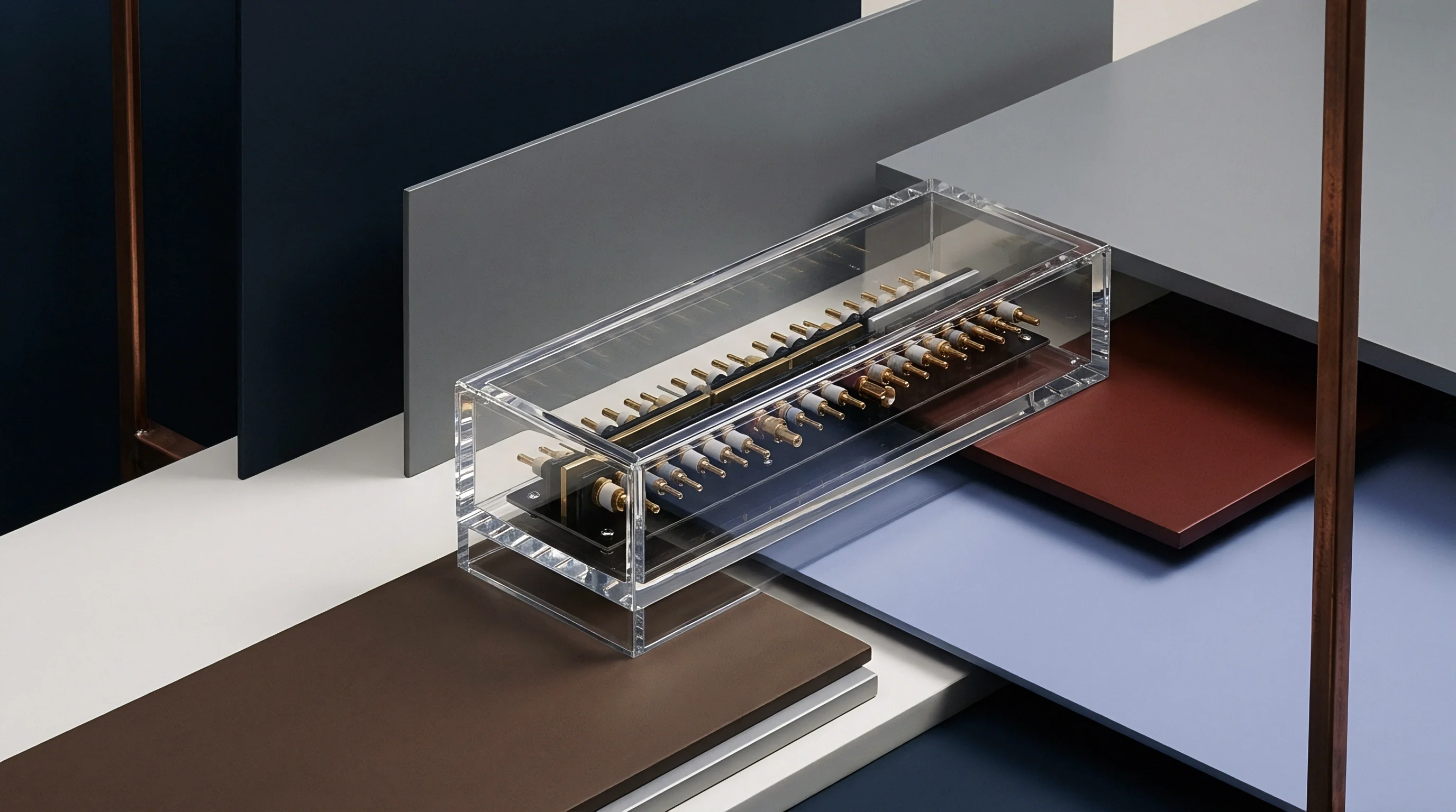
Standard surface-mount ceramic packages exhibit loop inductance proportional to the distance between their conductive end terminations. Smaller physical geometries shorten the internal current path, lowering equivalent series inductance. Standard 0805 components present approximately 1.0 nH of parasitic inductance, whereas 0402 footprints lower loop inductance to roughly 0.5 nH.
Reverse-geometry 0508 packages, which place terminations along the wide edge of the component, reduce internal inductance to 0.2 nH by widening the current flow path.
| Package Footprint | Physical Dimensions (mm) | Equivalent Series Inductance (nH) | Self-Resonant Frequency (100 nF Value) | Land Pattern Loop Inductance Addition (nH) |
|---|---|---|---|---|
| 1206 Standard | 3.2 × 1.6 | 1.25 | 14.2 MHz | 0.80 |
| 0805 Standard | 2.0 × 1.25 | 0.95 | 16.3 MHz | 0.60 |
| 0402 Standard | 1.0 × 0.5 | 0.45 | 23.7 MHz | 0.35 |
| 0508 Reverse Geometry | 1.25 × 2.0 | 0.18 | 37.5 MHz | 0.20 |
| 0603 Three-Terminal Feedthrough | 1.6 × 0.8 | 0.08 | 56.0 MHz | 0.10 |
Where Does Parasitic Loop Inductance Ruin Settling Time?
High-speed 24-bit converters experience severe conversion errors when board-level loop inductance exceeds two nanohenries, shifting the self-resonant point below the sampling frequency. Vias add parasitic loop inductance. Each standard PCB via contributes roughly 0.5 nH to 1.0 nH of inductance depending on barrel length and diameter.
Routing reference decoupling traces through multiple vias introduces high impedance at high frequencies, invalidating the low-impedance bypass network.
Placing local reservoir capacitors on the top assembly layer directly adjacent to reference IC ground pins minimizes loop area and maximizes ripple suppression performance.
Reverse geometry reduces component inductance. Board designers minimize loop area by placing surface-mount components on the top layer directly above a solid ground plane, using dual vias positioned in close proximity to reduce terminal loop area.
- Position the primary low-ESL ceramic component within two millimeters of the converter reference terminal.
- Route the ground return terminal directly to the converter analog ground plane using dedicated via pairs.
- Place wider PCB traces between the reference buffer output and the decoupling capacitor to minimize trace resistance.
- Isolate high-frequency digital clock signals from the reference decoupling loop using solid ground shield traces.
Shorter ground return loops always yield cleaner dynamic conversion spectra than larger capacitance values placed further down the trace.

Arithmetic
Designing a reference input decoupling network demands precise quantitative balancing of dynamic charge transfer, allowed voltage droop, and loop resonant frequency. Voltage drop scales with loop ESR. Calculating the required local storage capacity involves modeling the internal sampling array as a switched load during the acquisition phase.
Dynamic Charge Calculation for a 24-Bit SAR Converter
A successive approximation converter with a 100 pF internal capacitive DAC operating from a 5 V reference transfers 500 pC of dynamic charge during each sampling cycle. Assuming a target maximum allowable reference voltage droop equal to 0.25 LSB at 24-bit resolution, the peak permissible voltage disturbance equals 74.5 nV. The minimum external decoupling capacitance value required to supply this charge without buffer assistance is derived from the fundamental relation where capacitance equals charge divided by allowable voltage shift.
Dividing 500 pC by 74.5 nV yields a theoretical minimum capacitance of 6.71 mF. Placing a 6.71 mF capacitor directly on a precision reference node presents an impossible load for conventional reference buffers. Circuit designers overcome this by relying on the active reference driver to restore the charge balance within the acquisition window, allowing the physical decoupling capacitor value to be reduced to between 10 μF and 47 μF depending on buffer bandwidth.
| Decoupling Capacitance (μF) | Loop Inductance (nH) | Equivalent Series Resistance (mΩ) | Peak Voltage Dip (mV) | Settling Time to 0.5 LSB (ns) |
|---|---|---|---|---|
| 4.7 | 2.5 | 15 | 4.85 | 420 |
| 10.0 | 1.2 | 8 | 1.92 | 185 |
| 22.0 | 0.5 | 4 | 0.78 | 85 |
| 47.0 | 0.2 | 2 | 0.31 | 38 |
| Test Conditions: 24-bit SAR ADC, VREF = 5.0 V, CDAC = 100 pF, Acquisition Window = 200 ns. | ||||

Sensitivity Matrix for Voltage Droop and Settling Response
System designers calculate maximum permitted voltage disturbance based on the allowable bit-error budget assigned to reference instability. Impedance peaks mark series resonance. The total voltage drop at the reference pin equals the sum of the capacitive discharge droop, the resistive drop across equivalent series resistance, and the inductive spike across loop inductance.
An uncompensated voltage droop exceeding half a least significant bit during the acquisition window degrades system integral nonlinearity beyond datasheet guarantees.
- Capacitive Ratio Matching maintains the local reservoir value at least ten thousand times greater than the internal sampling array to bound voltage dip below 0.01 percent.
- ESR Bandwidth Control bounds maximum series resistance to prevent voltage spikes while providing sufficient real impedance to damp parasitic LC loop resonances.
- Dielectric Loss Budgeting accounts for insulation resistance drift over elevated operating temperatures to keep steady-state leakage currents below 50 nanoamperes.
- Thermal Dissipation Limits evaluate self-heating under continuous high-frequency conversion to ensure long-term capacitance stability.
IPC-2221A Clause 5.3.3 mandates minimum track clearances for precision analog nodes, altering board trace layout guidelines for high-voltage reference lines.
Verification
Validating reference node stability requires specialized impedance measurement techniques across a frequency range extending from tens of hertz to hundreds of megahertz. Shunt measurements isolate milliohm impedance. Standard single-ended oscilloscope probe setups introduce ground loop inductance that obscures sub-milliohm impedance characteristics and masks high-frequency ringing.

Two-Port Shunt-Thru Impedance Measurement Protocol
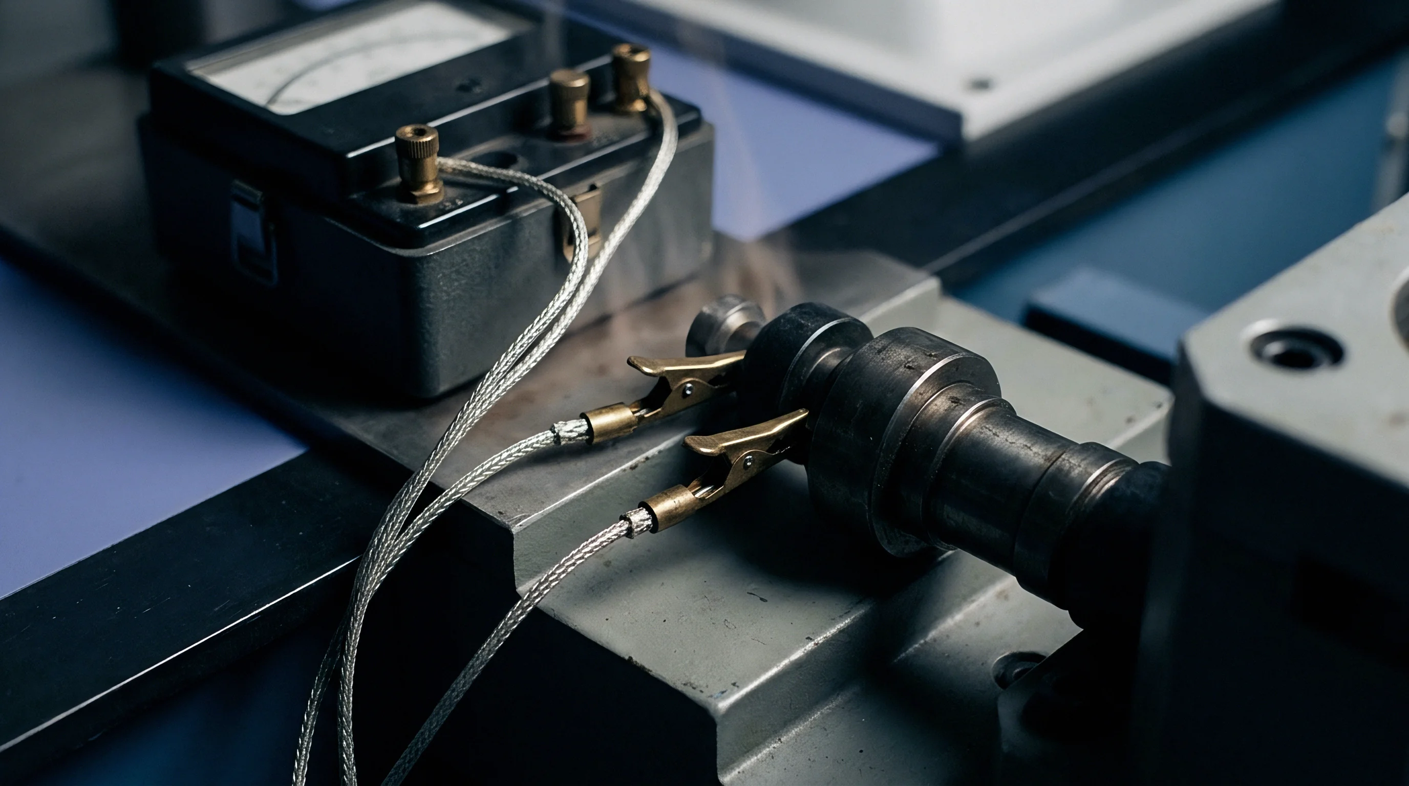
Measuring sub-milliohm impedance profiles at high frequencies necessitates coaxial cable connections configured to eliminate ground loop measurement errors. The two-port shunt-thru method connects port 1 and port 2 of a calibrated vector network analyzer in parallel across the decoupling component under test. This configuration suppresses braid loop currents, enabling accurate measurement of impedance levels down to 100 micro-ohms across frequencies from 10 kHz to 500 MHz.
- Vector Network Calibration eliminates coaxial cable parasitics and connector inductance down to a 100 micro-ohm noise floor across the entire measurement sweep.
- Active Transient Injection forces dynamic current steps into the reference node to record actual time-domain voltage recovery behavior under load.
- Baseband Noise Floor Mapping isolates low-frequency 1/f noise contributions from external dielectric microphonic pickup in high-gain front-end signal chains.
- Temperature Chamber Testing verifies impedance stability and dielectric absorption metrics across the specified industrial operating thermal envelope.

Time-Domain Transient Response and Spectral Noise Analysis
Capturing nanosecond voltage transients on reference pins demands high-impedance active probes paired with low-capacitance grounding accessories. Microphonic noise spoils low frequency accuracy. Combining time-domain transient testing with real-time FFT noise spectral density mapping isolates parasitic LC anti-resonance peaks caused by paralleling unequal capacitor values.
Paralleling a 10 μF X7R capacitor with a 100 nF C0G capacitor without accounting for package inductance creates a high-impedance anti-resonance peak at the frequency where the inductance of the larger component resonates with the capacitance of the smaller component. Operating the converter sampling clock near this anti-resonant frequency amplifies reference noise, inducing periodic code drops in the converter output spectrum.
Whether ultra-low-noise solid polymer tantalum devices can fully replace Class 1 ceramics in space-constrained 24-bit designs without introducing unacceptably high leakage current drift remains an active area of bench testing.
Sourcing
Procurement decisions for precision reference bypass capacitors balance dielectric performance metrics against unit pricing, lead times, and reel packaging formats. C0G dielectrics maintain constant value. High capacitance values increase reel cost.
High-density board designs frequently trade component unit cost against placement assembly yield when transitioning between standard chip footprints and advanced multi-terminal devices.
Commercial Dielectric Price Multipliers and Package Scaling
High-capacitance Class 1 C0G components in 1210 surface-mount footprints carry substantial cost premiums over Class 2 X7R equivalents of identical nominal value. A 10 μF 16 V C0G capacitor in a 1210 package commands a unit price roughly fifteen times higher than an equivalent X7R part. In production volumes reaching 100,000 units, component selection directly alters bill-of-materials cost, forcing sourcing teams to weigh pure C0G performance against managed X7R trade-offs.
| Component Architecture | Footprint Code | Dielectric Class | Unit Cost at 10k Volume (USD) | Standard Lead Time (Weeks) |
|---|---|---|---|---|
| Standard MLCC | 0402 | C0G | 0.04 | 8 |
| Reverse Geometry MLCC | 0508 | C0G | 0.18 | 14 |
| Three-Terminal Feedthrough | 0603 | X7R | 0.22 | 16 |
| High-Capacitance Precision MLCC | 1210 | C0G | 1.45 | 22 |
| Hermetic Polymer Tantalum | 7343 | Polymer | 2.10 | 18 |
Supply Chain Risks and Dual-Sourcing Qualification Rules
Securing secondary component sources prevents line shutdowns when specialty low-ESL ceramic formulations face long manufacturing lead times. Dual sourcing limits production lead times. Sourcing managers must verify that secondary qualified parts match primary components in dielectric class, package size, voltage rating, equivalent series resistance, and equivalent series inductance.
Substituting a qualified C0G part with a lower-cost Class 2 alternative during component shortages degrades analog conversion performance, generating field returns and qualification failures. Procurement specifications must explicitly lock dielectric chemistry and package physical layout to prevent unauthorized factory substitutions.
Volume packaging on 8 mm embossed carrier tape guarantees mechanical protection during high-speed automated placement, preserving solder terminal integrity across high-volume assembly runs.