Rolling Shutter Artifacts on a Moving Inspection Line
Rolling shutter inspection lines require pulsed strobe lighting within global overlap windows or native global shutter sensors to eliminate motion shear errors.


Readout
In automated vision systems, active-pixel CMOS sensors record spatial photon density over time to form images of moving items. Standard rolling shutter sensors expose and read out row by row, sweeping sequentially across the die rather than capturing every pixel simultaneously. When an object moves during this scan sequence, its position shifts between the top line’s exposure and the bottom line’s readout.
This timing lag across the pixel array converts physical motion into spatial distortion ~ skewing right angles, stretching vertical lines, and distorting circles into ellipses.
Conveyors running at 1.5 meters per second to 10 meters per second cause significant spatial displacement during frame capture. A standard two-megapixel sensor (1920 by 1080) with a 12.5-microsecond row readout requires 13.5 milliseconds to sweep from row zero to row 1079. An object moving across the focal plane at 4 meters per second advances 54 millimeters between the start of the top exposure and the end of the bottom readout.
In high-precision vision systems checking sub-millimeter tolerances, that offset displaces bounding boxes, breaks circle-fitting routines, and misaligns template matching masks.
Pixel architecture controls how photogenerated electrons gather and transfer to the output node. In classic three-transistor and four-transistor designs, photodiode integration links directly to row timing: resetting a line clears accumulated charge, exposure occurs for a set period, and the floating diffusion node samples voltage before the sensor steps down. The movement of an edge across successive line windows yields a predictable tilt angle ~ the arctangent of horizontal belt speed multiplied by row scan time, divided by vertical object pitch per pixel at the inspection plane.
At a belt speed of 5.0 meters per second and a line readout time of 9.6 microseconds per row, a 100-millimeter square target exhibits a 14.2-degree spatial shear angle across a 2048-row sensor array.
The underlying line rate directly controls the severity of this spatial skew.
Slower line rates increase horizontal displacement per row, exaggerating aspect ratio distortion along the direction of motion. In continuous web lines, foil rolling, and pharmaceutical vial inspection, these distorted profiles cause edge-detection algorithms to fail. Calculating part surface area by pixel count yields consistent errors as objects compress or stretch against the scan: moving counter to the scan compresses the silhouette, whereas moving in the scan direction elongates it.
Directional scanning shifts object centers of mass by up to 8.2 pixels in high-speed package tracking. That positional error propagates into calibration matrices, throwing off fixed-coordinate pick-and-place operations. When the controller receives shifted coordinates, end effectors miss targets, drop parts, or strike mechanical fixtures.
Correcting this offset generally requires linking encoder hardware directly to camera triggers, though line timing remains constrained by the sensor’s internal pixel clock.

Temporal Exposure Propagation across Active Arrays
Image capture on a rolling shutter sensor uses a sliding exposure window that moves line by line across the die. Each row delay adds a fixed phase offset relative to object movement, making exposure asynchronous across the frame. Photons hitting row zero record the object at time t0, while row N records it at t0 + N · trow.
This phase shift causes high-frequency frame vibrations to register as periodic ripples along vertical edges.
Micro-vibrations from motor bearings or loose belt guides interfere with the sensor’s fixed line frequency. When a belt vibrates at 120 Hertz against an 80 kilohertz row scan rate, physical movement modulates the horizontal edge position line by line, drawing wavy profiles along straight edges. Line-straightness routines interpret these visual artifacts as structural defects, triggering false rejections on high-speed lines.
| Sensor Vertical Resolution (Rows) | Row Readout Time (Microseconds) | Full Frame Readout Time (Milliseconds) | Conveyor Velocity (Meters/Sec) | Absolute Feature Shear (Millimeters) | Measured Distortion Angle (Degrees) |
|---|---|---|---|---|---|
| 1024 | 4.8 | 4.91 | 2.0 | 9.83 | 5.62 |
| 1024 | 4.8 | 4.91 | 5.0 | 24.57 | 13.81 |
| 2048 | 8.5 | 17.41 | 2.0 | 34.82 | 19.20 |
| 2048 | 8.5 | 17.41 | 5.0 | 87.04 | 40.97 |
| 4096 | 12.0 | 49.15 | 3.0 | 147.45 | 55.85 |
| 4096 | 12.0 | 49.15 | 8.0 | 393.22 | 75.72 |
Because line scans are sequential, the focal plane effectively samples object speed across time.
Total frame readout time caps the operating throughput of rolling shutter systems. Cutting individual row exposure times sharpens local edges but does not prevent overall geometric shear. A 10-microsecond line exposure produces clean edge segments, but the accumulated delay over 2000 rows still skews the overall image geometry.
Pulsed illumination fails to correct this warp if ambient lighting continues exposing pixels during the readout sweep.
- Line Clock Synchronization locks internal pixel clocks directly to quadrature encoder pulses from the conveyor drive shaft to establish hard timing references.
- Row-Phase Offset Compensation adjusts software inspection windows dynamically using belt speed data, compensating for spatial displacement across vertical rows.
- Region-of-Interest Windowing restricts row acquisition to a narrow vertical band around the part, cutting readout times from milliseconds to microseconds.
- Pulsed Strobe Gating triggers brief light pulses strictly during dark windows or global exposure overlaps to freeze object movement.
Integration duration remains the primary factor governing motion blur.
Choosing exposure parameters requires balancing signal levels against spatial clarity. Longer integration times gather sufficient light under standard factory illumination but increase edge blur as the part moves during row exposures. Shorter exposures demand high-intensity lighting to maintain signal-to-noise ratios, creating thermal management issues for continuous-duty fixtures installed over production lines.
The exact threshold where spatial un-warping algorithms introduce enough interpolation noise to degrade sub-pixel repeatability on flexible packaging remains uncertain.

Strobe
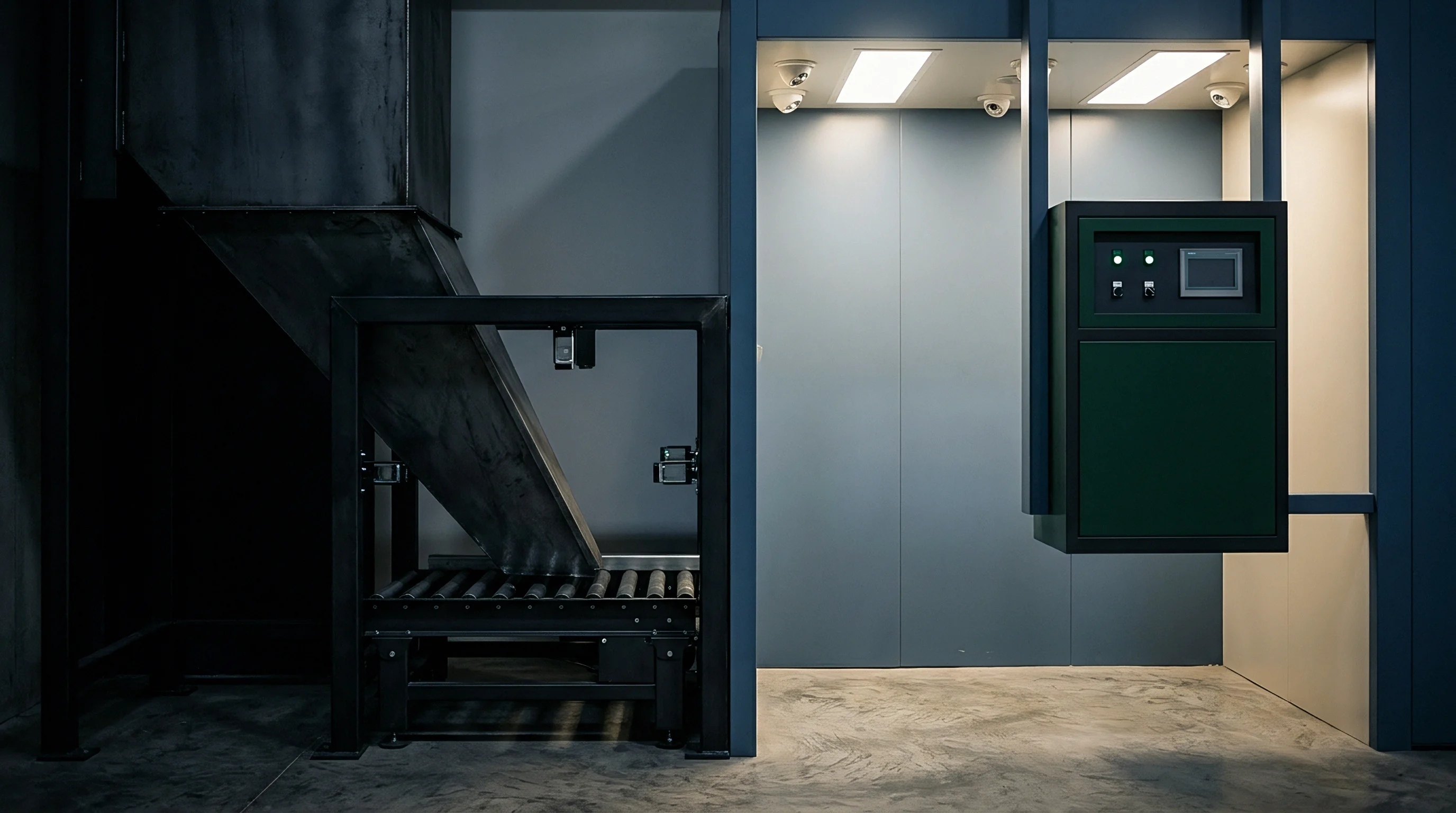
Pulsed LED illumination avoids rolling shutter distortion by decoupling exposure timing from line scanning. Inside dark enclosures that block ambient light, the sensor registers no background illumination during row sweeps. High-current LED arrays fire brief, intense light pulses, making effective exposure time depend on flash duration rather than row integration.
This freezes target motion at the instant of illumination, preserving sharp edges across varying belt speeds.
Synchronizing camera triggers with LED drivers demands low-jitter optocouplers and deterministic signal paths. Standard industrial outputs with 15 to 50 microsecond propagation delays can shift the flash out of alignment with the active exposure state. If a pulse fires while row zero is exposed but before line 2048 opens, lower regions stay unlit, creating truncated images that trigger false defect alarms.
Operational guidelines under ISO 12233 performance benchmarks dictate that strobe pulse duration must remain below the time required for an object to travel one-half of a pixel width across the image plane.
Global overlap modes create an operating window where every sensor row is exposed at the same time. Exposure starts at line zero and holds until the final row opens, integrating charge across the entire array simultaneously. Total exposure must exceed full-frame readout time, broadening the integration period.
Triggering the strobe strictly during this overlap window yields uniform exposure without geometric distortion, provided ambient light is low enough to prevent exposure during scan transitions.
- Overdrive Current Injection drives LED arrays at 300% to 800% of nominal continuous current in sub-millisecond bursts to maximize photon flux.
- Thermal Dissipation Limits restrict pulse duty cycles below 2% to prevent thermal degradation and spectral drift at emitter junctions.
- Jitter-Free Signal Propagation routes hardware triggers through field-programmable gate arrays over differential RS-422 lines instead of unshielded open-collector wiring.
- Global Overlap Phase Locking ties the strobe trigger directly to the camera’s flash output, ensuring activation only when all rows are actively integrating.
Properly timed strobing eliminates spatial shear completely.
LED spectral characteristics influence edge-detection performance on lines inspecting colored substrates or coated foils. Monochromatic red light at 630 nanometers provides high quantum efficiency on silicon photodiodes, whereas narrow-band blue light at 470 nanometers scatters better for detecting fine surface scratches on metal. Pulsing high-power white LEDs reveals phosphor lag: while the blue pump die reacts instantly, secondary yellow phosphor emissions decay over several microseconds, causing motion blur at higher line speeds.
Phosphor decay tails on consumer-grade white LED modules can exceed 18 microseconds during strobe testing. This persistent tail degrades trailing-edge contrast, softening boundaries on high-speed bottle inspection lines. Replacing commercial lighting with industrial multi-die monochromatic LED arrays eliminates phosphor persistence, producing sharp edge profiles that drop to zero intensity within 200 nanoseconds of trigger shutoff.

Illumination Synchronization Dynamics
High-speed strobe synchronization requires auditing the entire signal path across optical encoders, PLCs, vision processors, and LED drivers. Encoder pulses feed a motion controller that tracks part position from belt pitch. The controller sends a hardware trigger to the camera’s optoisolated input to initiate the scan sequence, and once internal flags confirm global exposure readiness, the camera’s dedicated flash output triggers the LED driver.
| Strobe Pulse Width (Microseconds) | LED Drive Current Multiplier | Effective Object Motion (Pixels at 5m/s) | Global Overlap Window Status | Illumination Uniformity Across Array | Edge Contrast Ratio |
|---|---|---|---|---|---|
| 2.0 | 8.0x | 0.08 | Verified Active | 99.2% | 45:1 |
| 10.0 | 4.0x | 0.40 | Verified Active | 98.8% | 42:1 |
| 50.0 | 2.0x | 2.00 | Verified Active | 95.1% | 28:1 |
| 200.0 | 1.0x | 8.00 | Partial Window Edge | 72.4% | 12:1 |
| 1000.0 | 1.0x | 40.00 | Overlap Mismatch | 38.9% | 4:1 |
Excessive readout times introduce progressive geometric skew.
Strobe timing windows shrink rapidly as belt speeds approach system limits. At 8 meters per second, a part travels 8 micrometers per microsecond. Maintaining sub-pixel repeatability on a setup with 20-micrometer optical resolution requires keeping illumination pulses under 2.5 microseconds.
Delivering pulses that short requires constant-current drivers capable of supplying 50-ampere spikes into low-impedance arrays with rise times under 100 nanoseconds.
- Strobe Trigger Latency Jitter occurs when controller software interrupts delay trigger pulses by microsecond intervals, pushing flashes outside the global exposure window.
- Phosphor Luminescence Lag stems from phosphor-converted white LEDs, leaving optical decay tails that generate motion blur along the line of travel.
- Ambient Light Leakage develops when ambient factory light enters inspection housings, exposing pixels during scan transitions regardless of strobe timing.
- Driver Voltage Collapse occurs when undersized LED power supplies sag under high-frequency pulse loads, diminishing flash intensity on successive parts and throwing off grey-level thresholds.
- Optocoupler Propagation Delay Dissimilarity happens when rising and falling edge delays drift over temperature, shifting strobe durations during extended operation.
Overall sensor die size directly drives manufacturing costs.
Dark-field shrouding around conveyor lines shields the inspection zone from ambient light variations. Housings with matte-black anodized interiors prevent strobe flashes from reflecting off structural frames into the optics. Eliminating external light forces the sensor to register exposure exclusively during the controlled microsecond pulse, freezing part geometry at the instant of illumination.
For moving lines, setting strobe pulse duration below the time required for a target to cross half a pixel width keeps motion blur well below the detection limits of sub-pixel edge routines.


Distortion
Geometric shear on rolling shutter sensors skews spatial dimensions in proportion to object velocity and row readout speed. A rectangle moving horizontally across the field registers as a parallelogram, with horizontal displacement accumulating line by line. Inspection algorithms checking circular stampings read this distortion as ovality, rejecting acceptable parts.
Reconstructing distorted frames in software demands real-time speed tracking, accurate line timing inputs, and considerable processing capacity.
Transformation matrices correct skewed images by shifting pixel rows horizontally based on line timing. The offset for row Y scales with the ratio of conveyor speed to optical resolution, adjusted by the time delay from the reference row. GPU software performs inverse affine transforms on raw frames before executing metrology algorithms.
This interpolation, however, smooths sharp boundaries, reducing sub-pixel edge accuracy by up to 35 percent compared to global shutter captures.
Machine vision systems operating under standard spatial calibration protocols suffer up to a 0.05-millimeter measurement error for every 1.0 meter per second increase in object speed when utilizing uncompensated rolling shutter sensors.
Photons generate charge at active pixel sites throughout exposure.
Mechanical vibrations overlaid on conveyor movement generate non-linear distortions that standard affine transformations cannot fix. Resonance from belt joints, drive chains, or compliant camera mounts introduces high-frequency ripples into the line readout. Straight vertical edges appear sinusoidal, causing linear edge-fitting routines to fail.
Resolving these distortions requires rigid mounting structures and vibration-damping isolators between the camera frame and conveyor assembly.
Determining exposure limits to eliminate motion shear requires careful analysis.
Determining the exposure limits needed to prevent rolling shutter shear involves comparing optical resolution to line speed. If a pixel covers 50 micrometers on the part, moving 50 micrometers during line readout shifts the image by a full pixel. Restricting spatial shear to a 0.1-pixel tolerance without strobing requires completing exposure before the part travels 5 micrometers.
At 2 meters per second, that limits total exposure time to under 2.5 microseconds.
Focal plane readouts introduce unavoidable timing delays.
Continuous web systems inspecting paper, film, or sheet metal experience distinct distortion patterns from rolling shutter sensors. Uniform web movement produces scaling errors rather than simple shear: moving opposite the scan direction compresses the image along the vertical axis, shrinking features, whereas moving with the scan stretches features vertically, distorting surface area and defect measurements.
On a high-speed battery foil line, an uncompensated rolling shutter camera mismeasured electrode coating gaps by 1.2 millimeters during speed transitions. The vision system passed three continuous coils with out-of-spec coating boundaries before a manual audit caught the error, scrapping $42,000 in processed lithium-ion electrode material. Replacing those rolling shutter units with native global shutter cameras featuring in-pixel storage resolved the measurement drift across all line speeds.

Mathematical Framework for Spatial Un-Warping Algorithms
Algorithmic correction reconstructs actual spatial coordinates (Xtrue, Ytrue) from distorted frame data (Xdistorted, Ydistorted). The distortion vector depends on row index Ydistorted and instantaneous velocity V(t). Assuming uniform horizontal speed V, spatial mapping follows a defined relationship based on sensor line time trow and magnification factor M in millimeters per pixel.
Spatial transformation operates according to the following mathematical relationship:
Xtrue = Xdistorted – left( fracV · trowM right) · Ydistorted
Ytrue = Ydistorted
| Conveyor Velocity (m/s) | Raw Edge Shear Error (Pixels) | Un-warping GPU Processing Time (ms/Frame) | Interpolation Sub-Pixel Loss (%) | Residual Measurement Error After Calibration (mm) |
|---|---|---|---|---|
| 1.0 | 3.2 | 0.45 | 8.2% | 0.012 |
| 2.5 | 8.0 | 0.48 | 14.5% | 0.028 |
| 5.0 | 16.0 | 0.52 | 22.1% | 0.055 |
| 7.5 | 24.0 | 0.61 | 31.4% | 0.092 |
| 10.0 | 32.0 | 0.74 | 38.7% | 0.145 |
Pixel pitch establishes baseline optical resolution.
Cycling ambient light compounds distortion when plant fixtures operate on AC power or high-frequency PWM. Fluorescent tubes and low-cost LED bays pulse output at 100 Hz, 120 Hz, or several kilohertz. As the rolling shutter scans under pulsing light, horizontal bands travel across the image, destabilizing grey-level thresholds and causing spurious edge detections, false defect flags, and inconsistent histograms.
- Linear Power Supply Conversion replaces PWM drivers with regulated DC supplies in inspection zones, eliminating light output ripple.
- High-Frequency Strobe Overdrive drives localized LED flashes to 20x ambient lux levels, making background intensity shifts negligible.
- Hardware Sensor Selection Adjustment replaces rolling shutter units with global shutter sensors when ambient light cannot be physically blocked.
Readout speed remains a major factor in image distortion.
Software correction relies on tracking speed fluctuations caused by belt wear or motor hunting. High-resolution optical encoders supplying tens of thousands of pulses per revolution allow the host system to update transformation matrices frame by frame. However, latency or polling jitter in encoder signals introduces speed errors into the algorithm, leaving residual distortion that degrades measurement accuracy on tight-tolerance parts.
Failing to isolate camera gantries from structural line vibration introduces high-frequency ripples that compromise sub-pixel measurement accuracy regardless of software corrections.

Wafer
Silicon architecture determines whether a sensor exhibits rolling shutter artifacts or captures global frame snapshots. Standard rolling shutter pixels use three-transistor (3T) or four-transistor (4T) designs that accumulate charge directly on the photodiode until row readout transfers it. Global shutter pixels add a fifth transistor (5T) and an isolated in-pixel memory node, allowing every pixel to integrate simultaneously before transferring charge into shielded storage for sequential readout.
Integrating an in-pixel storage node adds manufacturing complexity and reduces optical fill factor. Allocating die area to storage shrinks the photosensitive surface, lowering quantum efficiency unless micro-lenses concentrate light onto the active photodiode. Manufacturing 5T global shutter chips also requires extra masking steps during fabrication, reducing wafer yields and increasing costs relative to 3T or 4T rolling shutter designs of identical resolution.
Comparative bill-of-materials analysis reveals that global shutter image sensors carry a 3.5x to 5.0x price premium over equivalent-resolution rolling shutter sensors due to larger silicon die area and complex 5T manufacturing flows.
Global shutter dies command a substantial cost premium.
Parasitic Light Sensitivity (PLS) is a key benchmark for global shutter sensors operating in ambient light. It measures photon leakage into the in-pixel storage node during sequential readout after exposure completes. Poor PLS performance allows light entering during readout to corrupt stored charge, producing ghosting and vertical artifacts that resemble rolling shutter distortion.
Leading foundries insert tungsten shields within silicon metal layers to reach PLS extinction ratios better than 1:10,000.
| Pixel Architecture Type | Transistors Per Pixel | Relative Wafer Die Cost | Native Fill Factor (Without Micro-lenses) | Parasitic Light Sensitivity (PLS Ratio) | Motion Shear Susceptibility |
|---|---|---|---|---|---|
| 3T Standard Rolling Shutter | 3 | 1.0x | 78% | Not Applicable | High |
| 4T High Dynamic Range Rolling | 4 | 1.3x | 68% | Not Applicable | High |
| 5T Voltage-Domain Global Shutter | 5 | 3.8x | 42% | 1:5,000 | None |
| charge-domain Charge-Coupled Node | 6 | 4.6x | 35% | 1:20,000 | None |
| Stacked Back-Side Illuminated Global | 6+ (2 Die) | 7.2x | 88% | 1:50,000 | None |
Sensor bandwidth sets the baseline for frame throughput.
Back-side illuminated (BSI) stacked architecture overcomes fill-factor limitations in global shutter sensors. Placing the photodiode array on the top tier while moving storage nodes, control logic, and readout circuitry to a lower substrate connected by micro-bumps or through-silicon vias yields near 100% optical fill factors. Stacked sensors provide high quantum efficiency and low noise in compact footprints, though production remains limited to foundries running advanced 3D integration processes.
Sourcing strategy must weigh camera unit cost against downstream expenses for lighting, enclosures, and computing. Rolling shutter sensors lower initial camera hardware costs but require high-power strobes, low-jitter drivers, optical shrouding, and GPU processing to remove motion artifacts. Choosing global shutter cameras simplifies illumination and enclosure design, shifting expenditure into sensor hardware while reducing integration risk.
Second-source availability represents a major risk when deploying high-speed stacked global shutter sensors at scale. Proprietary pixel structures, unique pinouts, and custom LVDS or MIPI CSI-2 pinouts are frequently single-sourced from one foundry. If production halts or allocations shift, integrators face long lead times and redesign costs to adapt alternative components.
Specifying standard packages ~ such as 223-pin land grid arrays or one-inch C-mount compatible dies ~ preserves options across multiple vision hardware vendors. Securing secondary suppliers early in development protects lines against supply chain disruptions, allowing hardware swaps without redesigning mechanical mounts or updating drivers.
Standard procurement specifications for industrial vision systems require suppliers to provide certified line readout timing diagrams, parasitic light sensitivity ratings, and microsecond-level optocoupler latency figures before qualifying sensor hardware for high-speed applications.