Unintended Reactance
Unavoidable electrostatic coupling emerges between adjacent conductor geometries, ground planes and component pads across printed circuit board assemblies. Trace parasitic capacitance quantifies this unwanted distributed capacitive storage occurring along signal conductors separated by dielectric substrate materials. High-speed serial interfaces, high-impedance analogue front ends and sensor transducer nodes experience bandwidth limitations and signal degradation directly linked to this stray reactive element.
Physical trace width, conductor spacing, copper thickness and board dielectric constants dictate the magnitude of the resulting distributed capacitance. The parasitic effect ceases to be modeled as lumped capacitance when signal transmission wavelengths approach physical interconnect trace lengths, requiring transmission line analysis.
Dielectric Interactions
Electric fields propagate through the surrounding fiberglass resin matrix and soldermask layers, creating dielectric energy storage during signal transitions. The relative permittivity of the board material determines the magnitude of trace parasitic capacitance per unit of conductor length. Microstrip traces situated on outer board layers exhibit lower capacitive coupling to reference planes than stripline conductors embedded between inner ground planes.
Guard traces and coplanar ground fills provide electrical shielding, but they increase trace-to-ground capacitance if placed too close to sensitive conductor lines. Substrate manufacturing variations in dielectric thickness directly shift parasitic capacitance values across production runs.
Signal Degradation
Combining trace capacitance with source driver output resistance creates low-pass filtering networks that round off sharp digital switching edges. In high-speed sensor buses, trace parasitic capacitance extends signal rise and fall times, reducing valid data setup margins. High-impedance charge-output sensors such as piezoelectric accelerometers suffer direct signal attenuation when stray trace capacitance shunts generated charges to ground.
Differential signal paths experience common-mode conversion and timing skew when trace-to-ground capacitance values on complementary lines remain unbalanced. Layout design teams minimize trace lengths and remove copper ground planes beneath critical sensor pads to preserve analogue signal integrity.
Characterisation Protocol
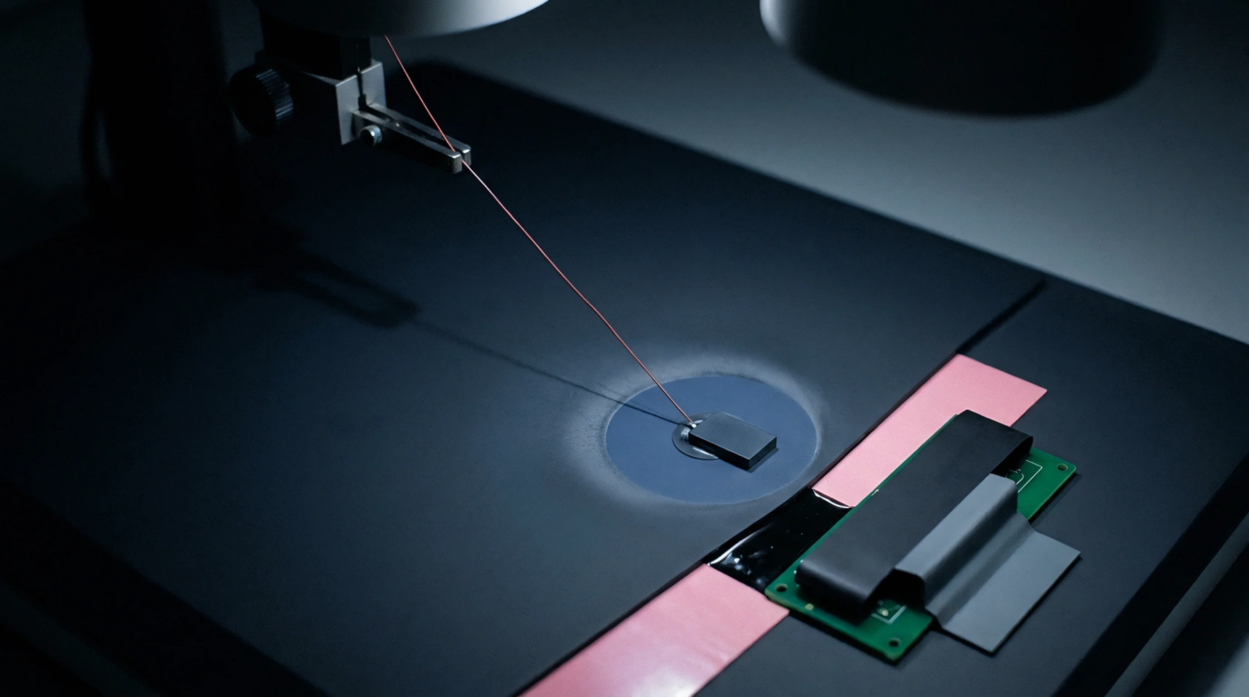
High-frequency impedance analyzers and time-domain reflectometers evaluate stray conductor capacitance during printed circuit qualification cycles. Time-domain reflectometry injects fast-step voltage pulses into the trace and calculates distributed parasitic capacitance from the reflected edge profile and propagation velocity. Electrical verification models compare measured capacitive parameters against electromagnetic simulation predictions to validate layout models.
Production quality assurance protocols monitor printed circuit dielectric constant tolerances and etching geometries to keep parasitic capacitance within defined circuit design limits. Managing unintended trace capacitance preserves measurement bandwidth and ensures dependable signal acquisition across high-precision electronic instrumentation.