Component Architecture
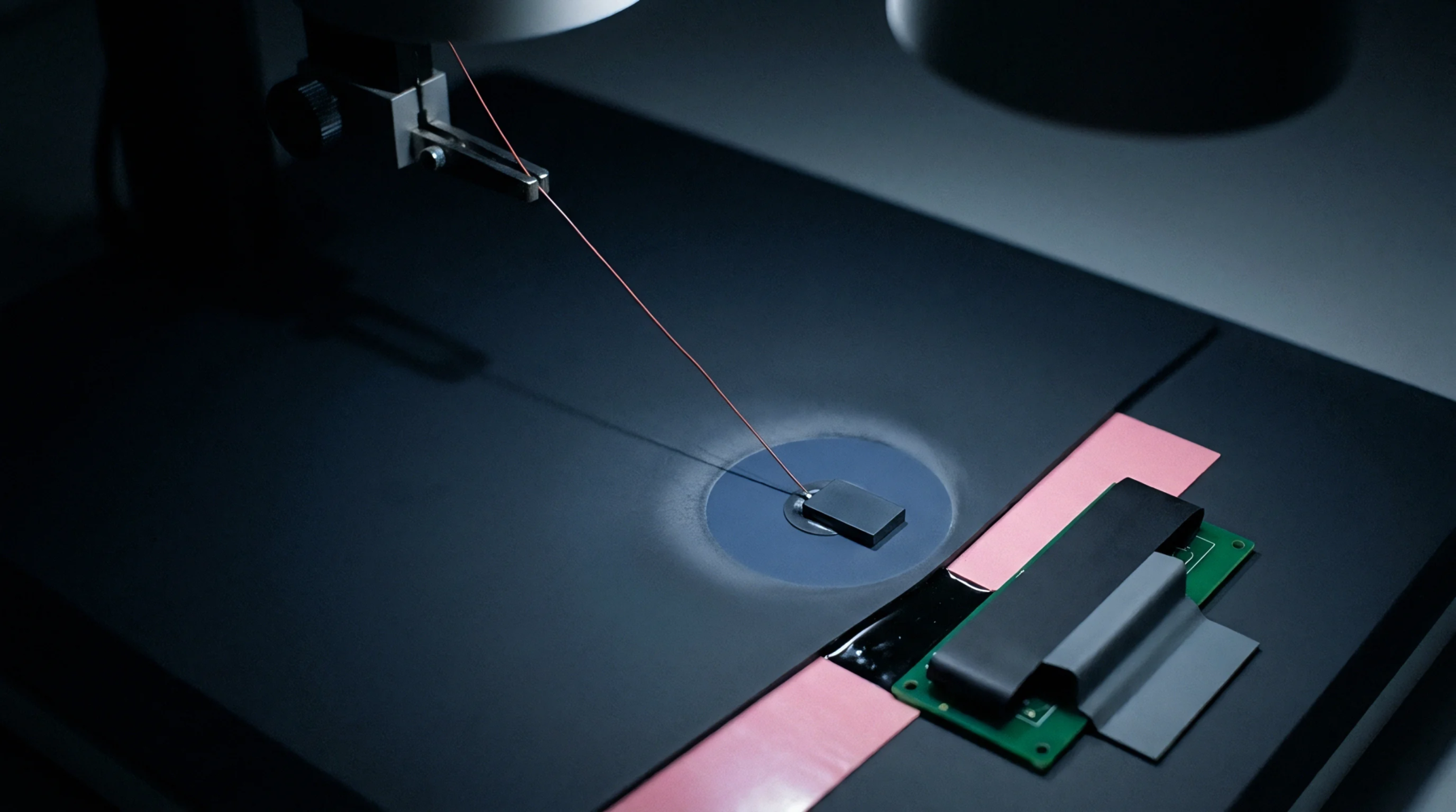
A quad flat no lead package provides a surface mount connection for integrated circuits by utilizing metallic pads on the bottom of the component body rather than extending external pins. Manufacturers design this physical structure to minimize the electrical path length between the semiconductor die and the printed circuit board. High frequency performance improves because parasitic inductance drops as the connection length decreases.
Thermal Conductivity
Copper lead frames within the quad flat no lead package act as heat dissipation paths for the silicon die. Efficiency of this cooling depends on the exposed thermal pad located underneath the main body. Solder joints bonding this pad to the board ground plane carry the bulk of the thermal energy away from the active junctions.
Engineers calibrate power dissipation limits based on the board copper area linked to this central thermal contact.
Assembly Tolerances
Precision in solder paste deposition dictates the formation of reliable joints along the perimeter pads. Misalignment during the reflow process alters the wetting geometry and increases the risk of short circuits between adjacent pads. Inspectors verify the standoff height between the component and the board surface to confirm that the mechanical stress on the solder remains within design parameters.
Automatic optical inspection systems track these dimensional variations to ensure high yields during mass production.
Calibration Constraints
Impedance matching of the connections requires consistent trace geometry on the host board to avoid signal reflections. Stray capacitance appears if the solder joint volumes vary between units during the heating cycle. Calibration cycles at the factory verify that the input and output lines remain stable under fluctuating temperatures.
Signal integrity reaches the intended limit when the board design accounts for the pad layout of the quad flat no lead package.