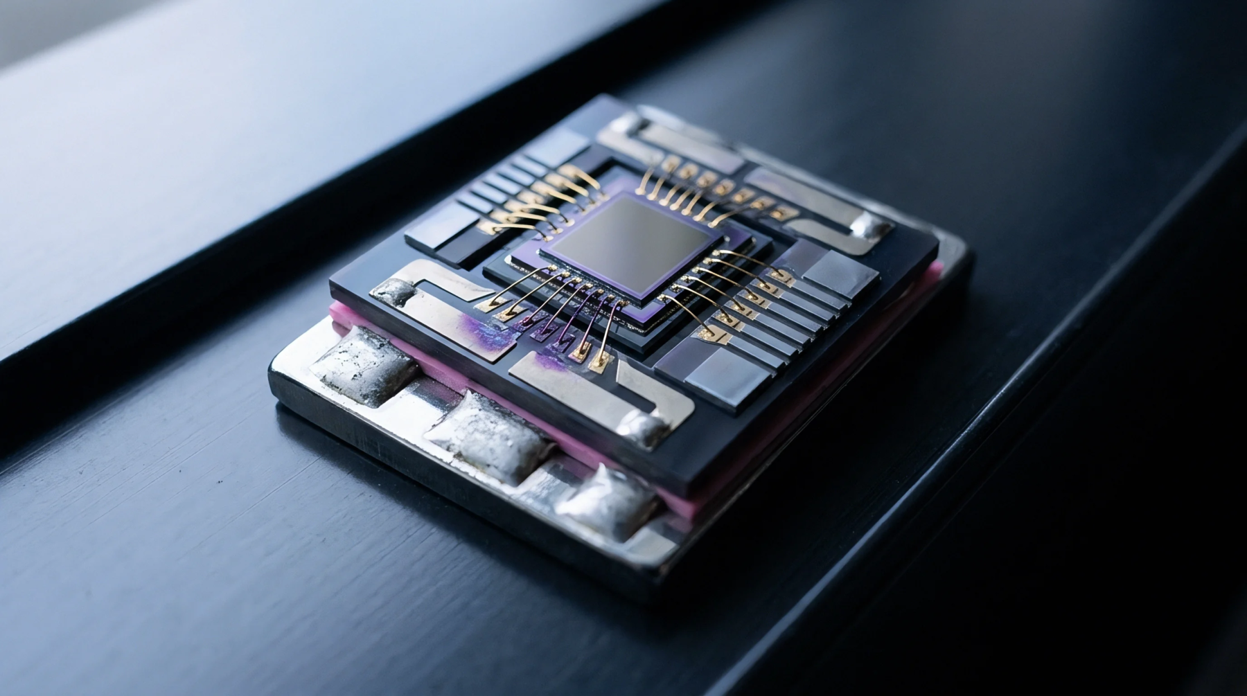
End of Life Notices That Take One Package and Spare Another
When component vendors end leaded packages, identical active silicon dies often survive in surface-mount forms that demand revised land patterns and thermal layouts.
Modified engineering cycles describe the process of repeating the physical layout and fabrication of a printed circuit board after errors are discovered in the initial prototype. This PCB re-spin becomes necessary when laboratory testing reveals logical flaws, unexpected electronic interference, or mechanical fit issues that cannot be solved by small hand-soldered jumpers. It involves returning to the original schematic files to adjust trace routes, move component footprints, or correct power plane layers that were causing signal noise or thermal bottlenecks.
The new design must then go through the full manufacturing sequence of mask creation, etching, and drilling to produce a new batch of refined hardware. Each revision adds to the total development time and costs associated with shipping a functional final product to the marketplace for industrial or consumer application.
Failures triggering this rework typically relate to high-speed signal integrity where trace lengths create timing mismatches that disrupt digital logic synchronization across the board surface. A PCB re-spin is also standard when clearance issues prevent the populated circuit from fitting into its specified housing or when heat dissipation proves insufficient for continuous power draws. Sometimes the choice follows an unexpected component obsolescence where a pin-compatible replacement is unavailable, forcing a change in the physical architecture to house a new silicon package.
Signal isolation problems where sensitive analog readings are corrupted by noisy digital clocks frequently lead to a redo of the internal ground plane strategy as well. Correcting these errors requires a deep review of current return paths to ensure that the second revision avoids the coupling problems found in the original prototype.
Repeating the layout and fabrication tasks generates significant expenses in engineering hours and physical manufacturing fees that reduce the overall profitability of the device program. For a successful board project, avoiding more than one PCB re-spin is a target for high-performing engineering teams who use extensive simulation and review logic before the first files are ever sent to the shop. Each iteration pushes the production schedule back by weeks or even months depending on the complexity of the board stack and the lead times at the external production facility.
High layer counts and specialized blind vias increase the financial pain of these events because the setup costs remain high for every separate release version of the artwork. Managing these risks involves rigorous checks of the bill of materials and mechanical fit models to ensure that everything aligns on the first physical arrival of hardware components.
Qualification of the second revision involves a repeat of the entire battery of electrical tests to confirm that the original problems are gone without creating new ones. During the PCB re-spin analysis, developers look at trace impedances and power delivery curves to verify that the changes reached their intended stability targets across the operating temp range. If the previous failure was purely mechanical, the check involves a simple assembly fit to ensure connectors line up with case holes correctly this time around.
This methodical verification step prevents the accidental release of partially functional hardware that could cause support issues in the field or lead to expensive recall actions later. A stable design signal at this stage finally marks the transition from engineering development to full scale mass production on the primary assembly lines.
When component vendors end leaded packages, identical active silicon dies often survive in surface-mount forms that demand revised land patterns and thermal layouts.
Expertise is a utility, not a secret. sentiention™ publishes its working knowledge as open reference: intelligence layer covering the materials it sources, the markets it enters, and the reference that serves both.