Planar Deformation
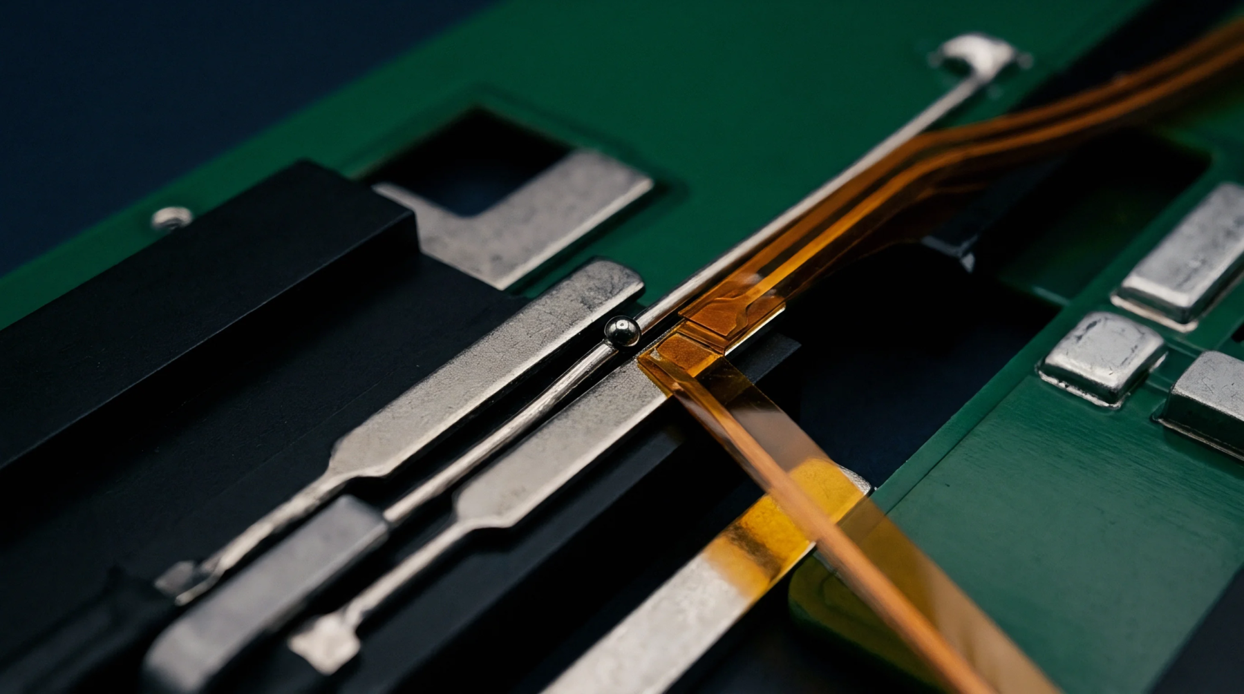
Maintaining a high degree of flatness is required for printed circuit boards to ensure proper assembly and reliable operation. This flatness requirement is quantified by IPC-A-610 substrate bow twist, which defines the maximum allowable deviation from a flat plane across the length and width of the board. The standard applies to both bare and assembled boards before they are mounted into their final enclosures.
Mechanical Stress
Asymmetrical copper distribution or thermal mismatches between laminates drive the distortion of the substrate during the manufacturing process. When the board is heated during soldering, these internal stresses cause the board to warp or twist. This physical deformation can strain soldered joints, leading to micro-cracks in the solder fillets or open circuits.
The risk of these failures increases with the size and thickness of the board.
Assembly Interference
Warped substrates present significant challenges to automated assembly equipment. Vacuum nozzles may fail to secure the board, and solder paste stencils may not make uniform contact with the surface. This poor contact results in uneven paste deposition and subsequent soldering defects.
Acceptance Threshold
Quality control personnel measure this deformation by placing the board on a precision surface plate and using a dial indicator or feeler gauges to find the highest point. The measured deviation is divided by the board length to calculate the percentage of warp, which must not exceed the limits specified in the IPC-A-610 standard. If the substrate bow twist exceeds the allowed limit, the board must be rejected or bake-flattened under pressure.
This verification step prevents mechanical failures in the field.