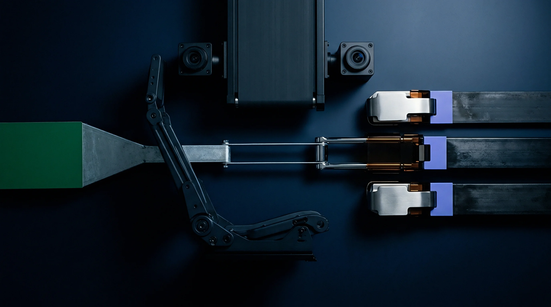
Solder Joint Geometric Variation
Solder joints formed during electronics surface-mount assembly frequently display geometric dissimilarity between opposing wetting faces or adjacent terminal sides. Such fillet asymmetry characterizes structural dimensional differences in meniscus curvature, joint height and wetting angles across discrete component terminations. It governs mechanical fatigue life, thermal expansion compliance and structural stability under high-vibration aerospace or industrial operating conditions.
The designation ceases to describe the connection if the solder volume drops below the minimum acceptable wetting threshold defined for non-wetted terminations.
Thermal and Wetting Imbalance
Differential thermal masses between asymmetric printed circuit board copper planes cause variations in regional reflow temperatures during soldering operations. Solder paste melts and flows faster toward the higher-temperature terminal, while delayed wetting on the colder land pattern generates an uneven meniscus. Capillary action draws liquid alloy unevenly if solder mask clearances, terminal plating thicknesses or component pad geometries lack symmetry.
Oxidation on individual component terminations compounds this effect by hindering intermetallic compound development across sluggish wetting interfaces. Uneven pad dimensions alter the equilibrium wetting balance, pulling the component off-centre or producing unequal meniscus heights between opposing electrical leads.
Mechanical Strain Concentration
Unequal joint profiles create irregular shear stress gradients across solder terminations during thermal cycling intervals. Thinner solder fillets experience early mechanical fatigue cracking due to concentrated strain energy under cyclic thermal expansion differences between ceramic packages and FR4 laminates. Severe fillet asymmetry induces package tilt that perturbs high-frequency line impedance, optical sensor alignments and mechanical clearance envelopes inside compact enclosures.
Automated optical inspection tools monitor joint profiles to capture geometric anomalies before cracked solder joints produce field failures.
Optical Inspection Measurement
Automated three-dimensional optical inspection stations map solder volume and profile elevations on finished printed circuit board assemblies. Laser triangulation and structured fringe projection extract surface coordinates to reconstruct the three-dimensional curvature across every termination. Inspection software calculates the ratio of wetting height to fillet thickness on each side and checks adherence to IPC-A-610 acceptability criteria.
Deviations exceeding structural balance limits require solder paste volume adjustment, reflow thermal profile modification or board layout redesign.