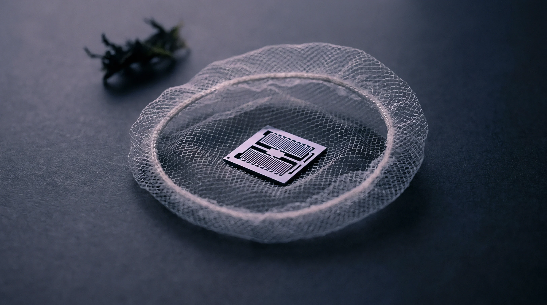
Doping Technology
Semiconductor fabrication relies on the introduction of select impurities to modify electrical conductivity. Boron implantation represents a high-energy process where ionized boron atoms are accelerated into silicon wafers to form p-type regions. The physical boundaries of this process are defined by the acceleration voltage and the dose of ions delivered.
Physical Mechanics
Silicon crystal matrices are modified when high-speed boron ions collide with lattice atoms. This bombardment during boron implantation creates atomic displacements, which require subsequent high-temperature annealing to restore the silicon crystal structure and activate the dopants. The electrostatic scanner deflects the beam to ensure a uniform distribution across the entire surface of the semiconductor wafer.
Drift in beam current during this phase directly degrades the precision of the resulting sheet resistance.
Metrological Verification
Ion beam current is verified before each wafer run using an integrated Faraday cup positioned behind the wafer plane. In secondary ion mass spectrometry, the dose is profiled to confirm that the peak concentration matches the target specification within a pre-defined tolerance. This laboratory technique uses a sputtering beam to measure depth-resolved concentrations.
Any mismatch in the primary ion energy alters the depth profile, shifting the junction depth and affecting the threshold voltage of the completed semiconductor device.
Process Limitation
Electrostatic charging of the insulating surfaces represents a significant challenge during this operation. Shielding systems use plasma flood guns to neutralize build-up and prevent dielectric breakdown.