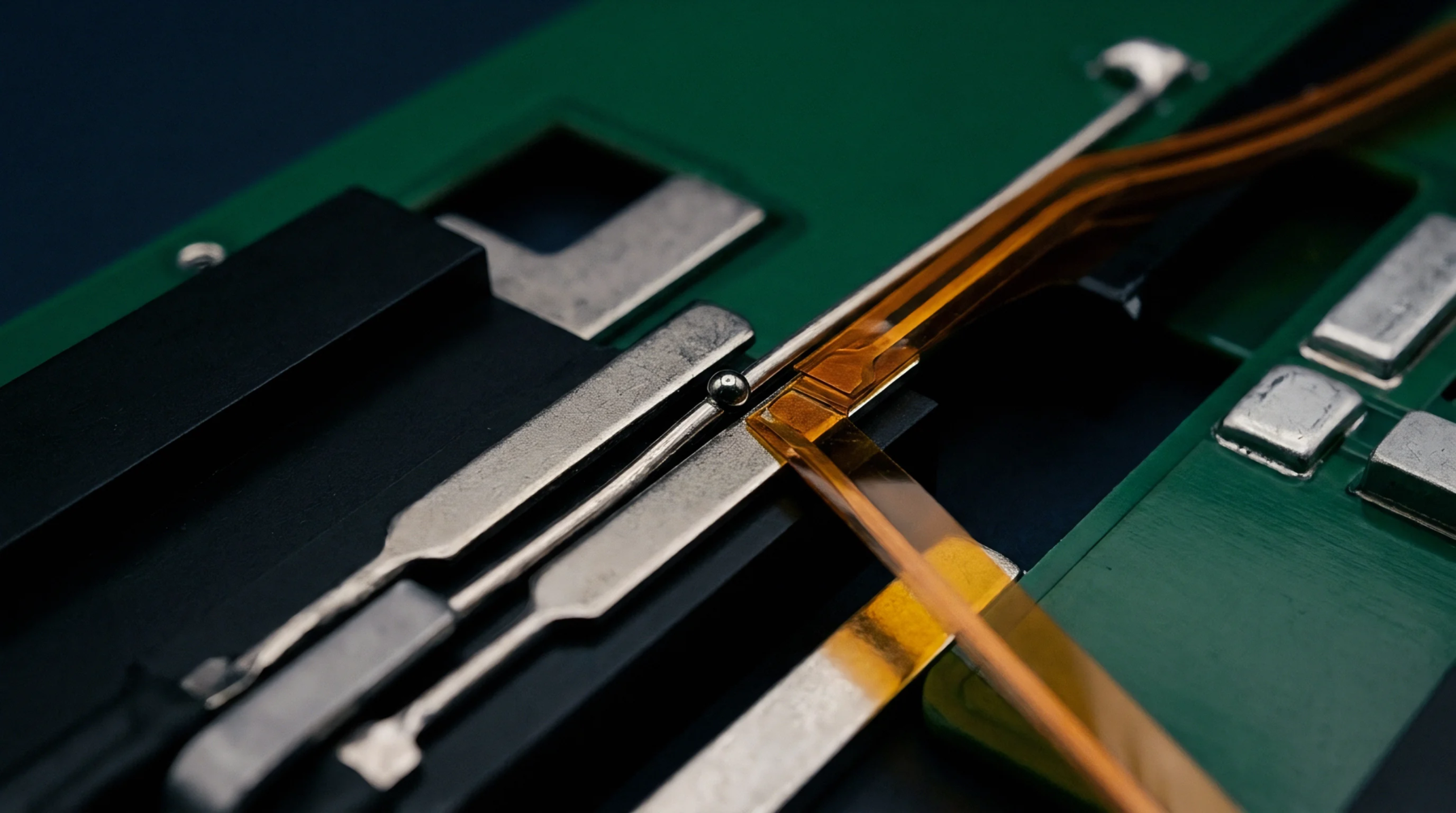
Dielectric Isolation Layer
Thin-film ceramic passivation coatings prevent ionic diffusion and electrical breakdown across microelectronic sensor assemblies. Within high-temperature sensing packages, an aluminum oxide barrier isolates conductive traces from reactive atmospheres or conductive structural substrates. The layer is verified through dielectric breakdown voltage testing under elevated thermal environments.
Electrical insulation fails if pinhole defects or micro-cracks form during thermal cycling.
Deposition Methodology
Chemical vapour deposition and atomic layer deposition provide conformal film coverage across fine sensor features. The aluminum oxide barrier coats complex aspect ratios without creating pinholes or uneven thickness variations across contact steps. Sputtered films can develop directional shadowing, leading to localized regions of reduced dielectric protection.
Mechanical stress within thicker layers risks micro-cracking during rapid temperature changes. The boundary of protection stops when structural spallation occurs under extreme thermal shock.
Degradation Mechanism
High-temperature environments accelerate ion migration across thin dielectric films. In the presence of moisture or alkali contaminants, an aluminum oxide barrier experiences localized leakage current increases. Oxygen vacancy formation under continuous electrical field bias alters the insulation properties over extended operational lifespans.
Trace chemical reactions with substrate silicon can produce intermediate silicate phases that degrade boundary cohesion. Qualification protocols measure this breakdown via accelerated lifetime testing at maximum operating temperature.
Metrological Verification
High-potential insulation testing confirms that leakage current remains below specified microampere limits at rated operating voltages. When evaluating an aluminum oxide barrier, metrology laboratories test insulation resistance using four-point probe structures across temperature ramps. Factory acceptance requires verification of dielectric permittivity against certified reference materials.
The layer specification governs sensor stability by preventing parasitic parallel resistance paths from distorting primary transducer outputs.