Assembly Stress
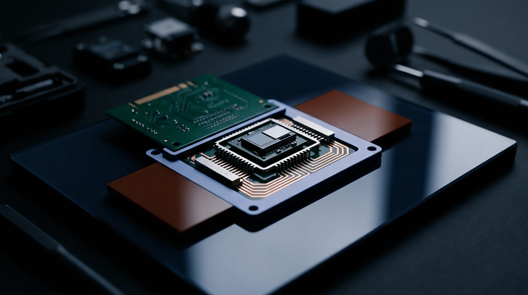
Force exerted by a printed circuit board on a wafer level chip scale package causes measurable changes in device performance. This wlcsp mounting strain arises because the component is soldered directly to the board without a protective plastic housing. The difference in thermal expansion between the silicon and the substrate creates this mechanical tension.
Electrical Impact
Stress sensitive circuits such as precision references and amplifiers experience an offset shift when the board flexes. Because wlcsp mounting strain is transmitted through the solder bumps, the layout of the bumps affects the magnitude of the error. Components positioned near the center of a board often experience different stress levels than those near the edges.
Mitigation
Underfill materials are sometimes applied between the die and the board to redistribute the mechanical load. Without this support, wlcsp mounting strain can lead to solder joint fatigue or silicon cracking during thermal cycling. Board designers must also avoid placing large components or mounting screws near sensitive chip scale devices.
Calibration
Systems that require high accuracy must be calibrated after the assembly is complete to remove the errors introduced by the board. Testing at the module level is the only way to verify the final performance.