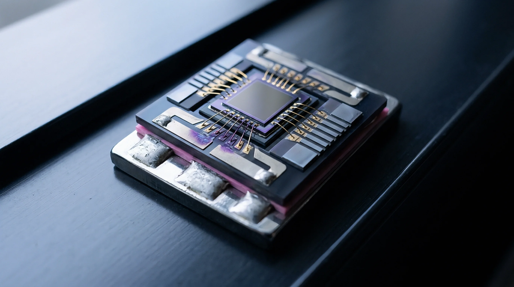
End of Life Notices That Take One Package and Spare Another
When component vendors end leaded packages, identical active silicon dies often survive in surface-mount forms that demand revised land patterns and thermal layouts.
Geometric dimensions define the center to center distance between adjacent leads or pads on an integrated circuit package or a printed circuit board. The pin pitch is a critical parameter that dictates the density of the electronic assembly and the required precision of the manufacturing equipment. In the early days of electronics, a pitch of two point five four millimeters was the standard for through hole components.
As the demand for smaller devices grew, the industry moved to surface mount packages with pitches of one point two seven millimeters, then zero point eight millimeters and now as low as zero point four millimeters. This reduction in spacing allows more functionality to be packed into a smaller area, but it also creates significant challenges for the design and assembly processes. The choice of pitch is a balance between the need for miniaturization and the limitations of the soldering and inspection tools.
Layout of the printed circuit board must accommodate the specific spacing of the component pins to ensure reliable electrical connections. A finer pitch requires thinner copper traces and smaller gaps between them, which increases the complexity and the cost of the board fabrication. If the traces are too close together, there is a risk of electrical shorts or signal interference between the adjacent lines.
Designers must also leave enough room for the via holes that connect the different layers of the board. For high pin count devices such as ball grid arrays, the pitch is so tight that it requires advanced techniques like microvias and build up layers. The pin pitch also determines the type of solder stencil and the size of the solder balls used during the assembly process, with smaller dimensions requiring more careful control of the paste volume.
Manufacturing success for fine pitch components depends on the accuracy of the pick and place machine and the stability of the reflow process. A small misalignment of only a few microns can cause the pins to miss their pads or to bridge across to a neighbor, creating a defective joint. To prevent these errors, automated optical inspection systems are used to check the position of every part before it goes into the oven.
The solder paste must also be formulated with a specific grain size to ensure it flows correctly through the tiny openings of the stencil. As the pitch becomes smaller, the mechanical strength of the individual solder joints decreases, making the assembly more susceptible to damage from vibration or thermal stress. This necessitates the use of underfill materials or more robust package designs to protect the delicate connections.
Evolution of the pin pitch is a primary driver of the constant decrease in the size of consumer electronics such as smartphones and tablets. However, there is a physical limit to how close the pins can be placed before the manufacturing yield becomes unacceptably low. Below zero point three millimeters, the risk of solder bridging and the difficulty of inspecting the joints become major barriers.
The industry is responding by moving toward leadless packages and wafer level technologies that eliminate the pins entirely in favor of flat pads. Despite these trends, the pin pitch remains a fundamental specification that every electronics engineer must understand and manage. It is the bridge between the silicon chip and the rest of the system, defining the physical interface of the modern electronic world.
When component vendors end leaded packages, identical active silicon dies often survive in surface-mount forms that demand revised land patterns and thermal layouts.
Expertise is a utility, not a secret. sentiention™ publishes its working knowledge as open reference: intelligence layer covering the materials it sources, the markets it enters, and the reference that serves both.