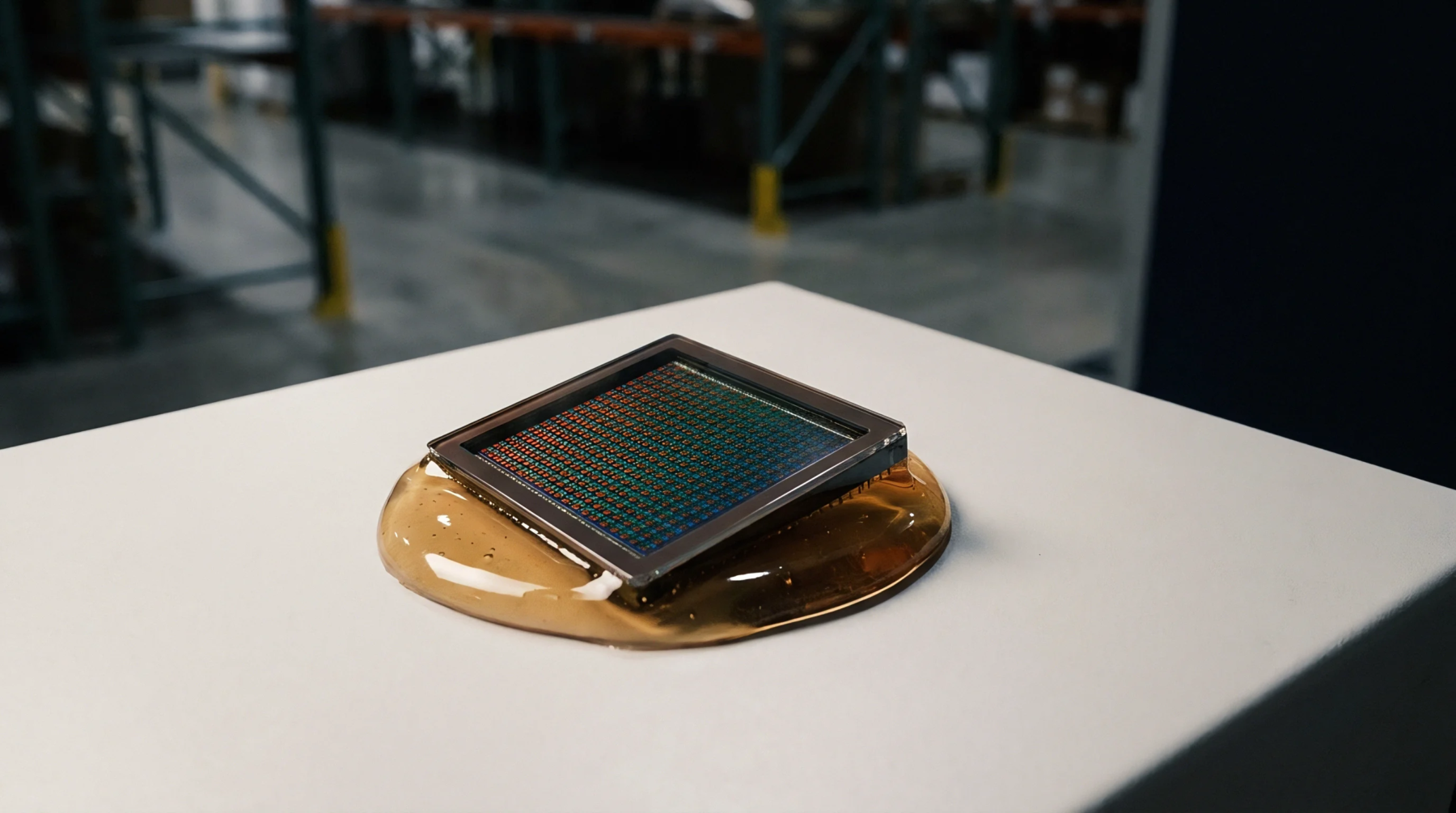
Quantifying Viscoelastic Adhesive Stress Relaxation in Ceramic LCC Sensor Packages
Viscoelastic adhesive relaxation in ceramic LCC packages causes time-dependent zero drift, requiring master-curve Prony modeling to quantify long-term offset shift.
Intermediate structural platforms bridge the coefficient of thermal expansion divergence between delicate semiconductor sensing dies and coarse organic printed circuit boards. An interposer submount provides high-density routing, mechanical stress isolation, and thermal dissipation pathways within miniature sensor package architectures. Materials such as silicon, alumina, aluminum nitride, or glass are engineered with matched thermal expansion values to protect delicate microelectromechanical systems from mechanical package warpage.
Modern MEMS pressure sensors, micro-mirrors, and optical transceivers rely on these structures to maintain absolute mechanical positioning and signal fidelity under severe operational vibrations.
The primary operational mechanism relies on absorbing the high thermomechanical strain that develops between high-expansion substrate laminates and low-expansion semiconductor elements. Solder balls or copper pillars connect the submount to the printed circuit board, taking up the bulk of shear strain during rapid thermal cycling. The rigid submount ensures that the sensor die mounted on its upper surface experiences a minimal strain field, preventing localized micro-cracking of active silicon structures.
Fine through-wafer vias within the submount transfer high-frequency electrical signals directly from top bonding pads to bottom arrays, minimizing parasitic inductance and capacitance. Precise planar geometries prevent tilting of optically sensitive detectors, preserving line-of-sight alignments over wide thermal ranges.
Dimensional tolerances for micro-machined silicon and ceramic submounts fall within micrometer and sub-micrometer boundaries to ensure reliable flip-chip die alignment. Wafer-level lithography forms fine-pitch conductor tracks, while deep reactive-ion etching or laser drilling generates smooth, high-aspect-ratio vertical interconnections. Thin-film deposition processes lay down barrier and seed layers such as titanium-tungsten and gold to facilitate void-free solder wetting during assembly.
Solder volume consistency across all bonding pads remains mandatory to eliminate differential tilting and residual package tilt. Die shear strength inspections evaluate interfacial bond adhesion, discarding production lots showing incomplete intermetallic formation or micro-voiding. Sourcing contracts stipulate strict surface planarity and roughness values to avoid stress concentration nodes across brittle sensor membranes.
Structural utility ends where thermal dissipation requirements exceed the intrinsic thermal conductivity of the chosen interposer material. Selecting high-conductivity substrates like aluminum nitride addresses high-power electronic challenges but incurs significant raw material and processing cost premiums. Package designers must trade off the added assembly height and package complexity against the operational isolation benefits provided by the submount.
Piezoresistive pressure devices utilize submounts to arrest assembly stresses that otherwise manifest as zero-point offset errors, whereas pure capacitive sensors may prioritize dielectric losses across the platform. Verification procedures confirm that the chosen package submount tolerates the maximum specified solder reflow temperatures without delaminating internal metal-filled vias.
Viscoelastic adhesive relaxation in ceramic LCC packages causes time-dependent zero drift, requiring master-curve Prony modeling to quantify long-term offset shift.
Expertise is a utility, not a secret. sentiention™ publishes its working knowledge as open reference: intelligence layer covering the materials it sources, the markets it enters, and the reference that serves both.